Detection mechanism and detection device

A detection mechanism and detection device technology, applied in the fields of semiconductor/solid-state device testing/measurement, electrical components, semiconductor/solid-state device manufacturing, etc., can solve the problems of high cost and low detection efficiency, so as to reduce the detection cost and improve the detection effect. , clear imaging effect

Pending Publication Date: 2019-10-25
WUXI AUTOWELL TECH
View PDF0 Cites 2 Cited by
  • Summary
  • Abstract
  • Description
  • Claims
  • Application Information

AI Technical Summary

Problems solved by technology

[0003] The traditional detection method can only detect one of the faces of the detected edge, which has low detection efficiency and high cost

Method used


Image

  • Detection mechanism and detection device
  • Detection mechanism and detection device
  • Detection mechanism and detection device

Examples


no. 1 example

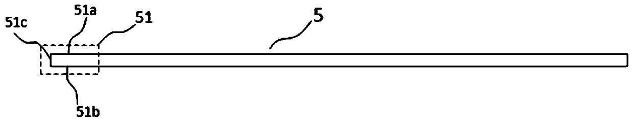
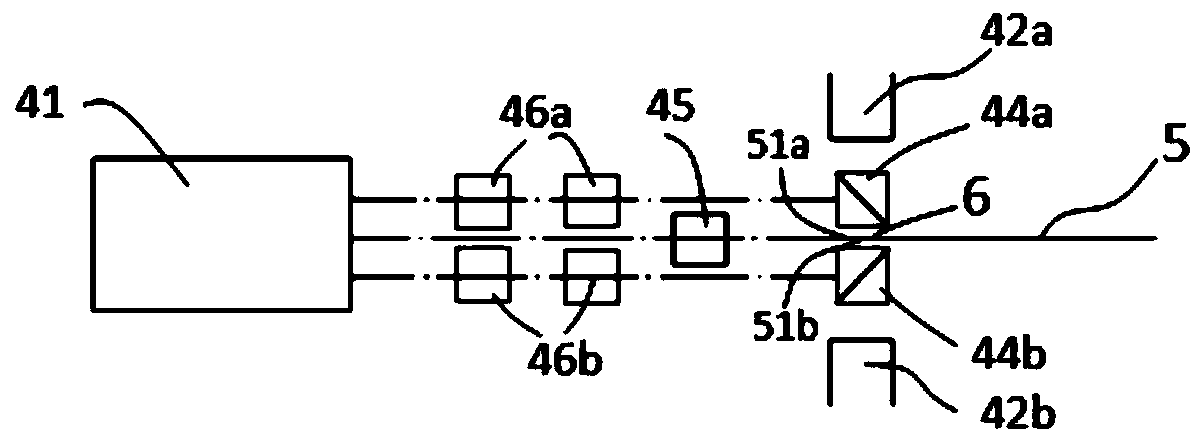
[0048] like figure 2 , image 3 As shown, the plane where the detection station 6 mentioned in this embodiment is located is parallel to the horizontal plane. Correspondingly, the silicon wafer 5 to be tested located at the detection station 6 is also in a horizontal state, the first surface of the tested edge 51 of the silicon wafer 5 to be tested is the upper surface 51a, and the second surface of the silicon wafer 5 to be tested is the lower surface 51b.

[0049] The surface light source includes an upper surface light source 42a and a lower surface light source 42b, and the surface reflection mechanism includes an upper surface reflection mechanism 44a and a lower surface reflection mechanism 44b. in:

[0050] The upper surface light source 42a is located above the detection station 6, the upper surface light source 42a is configured to emit upper surface irradiation light to the upper surface 51a of the edge to be tested 51, and the upper surface reflection mechanism ...

no. 2 example

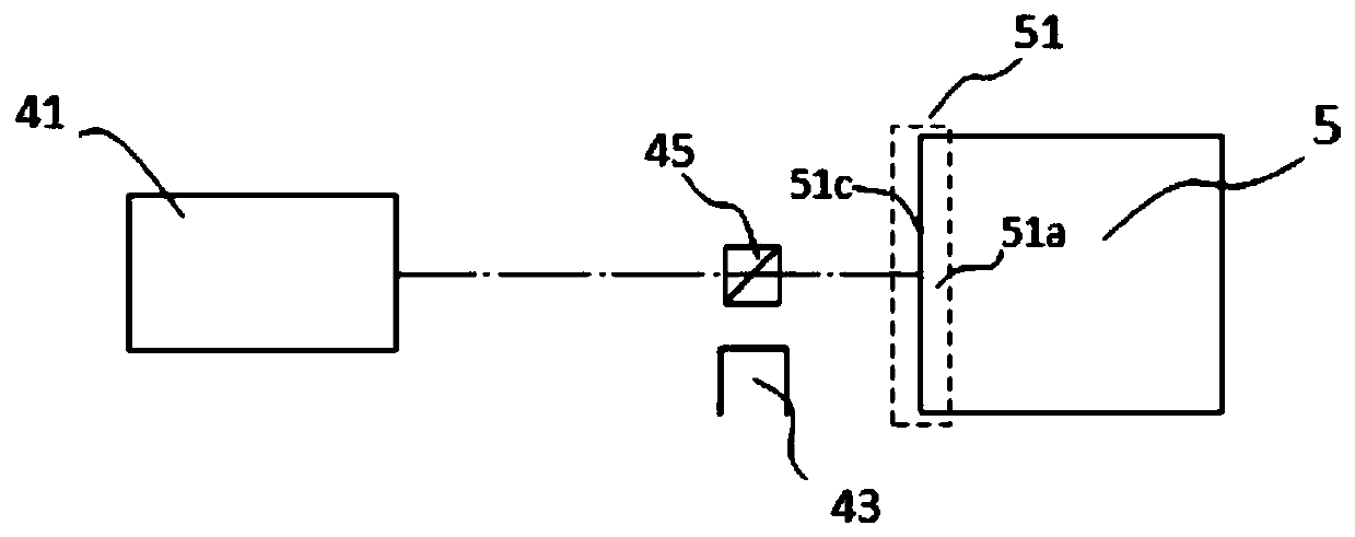
[0065] like Figure 4 As shown, the structure of the detection mechanism provided in this embodiment is basically the same as that of the detection mechanism in the first embodiment. The only difference between the two is that in the first embodiment, the first cylindrical lens 46 a and the second cylindrical lens 46 b are arranged close to the detection camera 41 . However, in this embodiment, the first cylindrical lens 46 a and the second cylindrical lens 46 b are arranged close to the detection station 6 .

no. 3 example

[0067] like Figure 5 As shown, the structure of the detection mechanism provided in this embodiment is basically the same as that of the detection mechanism in the first embodiment. The only difference between the two is that in the first embodiment, the number of the first cylindrical lens 46 a and the number of the second cylindrical lens 46 b are both two. However, in this embodiment, the number of the first cylindrical lens 46a and the second cylindrical lens 46b is one.


PUM


Abstract

The invention provides a detection mechanism used for detecting a tested edge of a to-be-tested silicon at a detection station, the tested edge includes two opposite first surfaces, a second surface and an end surface connecting the first surfaces and the second surface. The detection mechanism includes a surface light source, an end surface light source, a surface reflection mechanism, an end surface reflection mechanism and a detection camera, wherein the surface light source is configured to illuminate surface illumination light to at least one surface of the tested edge, the surface reflection mechanism is configured to reflect the surface illumination light reflected by the at least one surface to the detection camera, the end surface reflection mechanism is configured to reflect theend surface illumination light emitted by the end surface light source to an end surface of the tested edge, and the end surface illumination light is reflected by the end surface of the tested edge to the detection camera. The detection mechanism is advantaged in that the end surface of the tested edge of the to-be-tested silicon and at least one surface can be detected, and thereby detection efficiency is improved, and detection cost is reduced.

Description

technical field [0001] The invention belongs to the field of silicon wafer detection, and in particular relates to a detection mechanism and a detection device. Background technique [0002] In the production process of solar cells, silicon rods need to be cut into silicon wafers first, and then the silicon wafers need to be cleaned. After cleaning, the silicon wafers need to be inspected. Generally, the silicon wafer is placed on the conveying device, and the detection devices are installed on both sides of the conveying device to detect the dirt, hidden cracks, edge defects, warpage, etc. of the two edges of the silicon wafer parallel to the conveying direction. like figure 1 As shown, a measured edge 51 of the silicon wafer 5 includes three surfaces, namely: an opposite upper surface 51a and a lower surface 51b and an end surface 51c connecting the upper surface 51a and the lower surface 51b. [0003] The traditional detection method can only detect one side of the dete...

Claims


Application Information

Patent Timeline
Patent Type & Authority Applications(China)
IPC IPC(8): H01L21/66H01L21/67
CPCH01L21/67242H01L21/67288H01L22/12H01L22/20
Inventor 李文李昶徐飞李泽通马红伟
Owner WUXI AUTOWELL TECH
Why Eureka
Try Eureka