

A power semiconductor module packaging structure
A power semiconductor and module packaging technology, which is applied to semiconductor devices, semiconductor/solid-state device components, electric solid-state devices, etc., can solve the problems of lower product yield and lower reliability of power semiconductor modules, and achieve simplified production process and quantity Reduction, good effect of economy
- Summary
- Abstract
- Description
- Claims
- Application Information
AI Technical Summary
Problems solved by technology
Method used
Image

Examples
Embodiment Construction
[0030]The implementation of the present invention will be described in detail below in conjunction with the accompanying drawings and examples, so as to fully understand and implement the process of how to apply technical means to solve technical problems and achieve technical effects in the present invention. It should be noted that, as long as there is no conflict, each embodiment and each feature in each embodiment of the present invention can be combined with each other, and the formed technical solutions are all within the protection scope of the present invention.
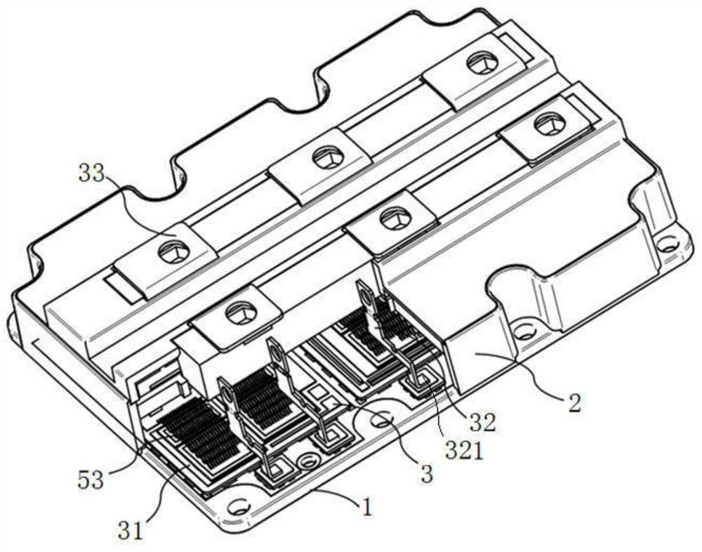
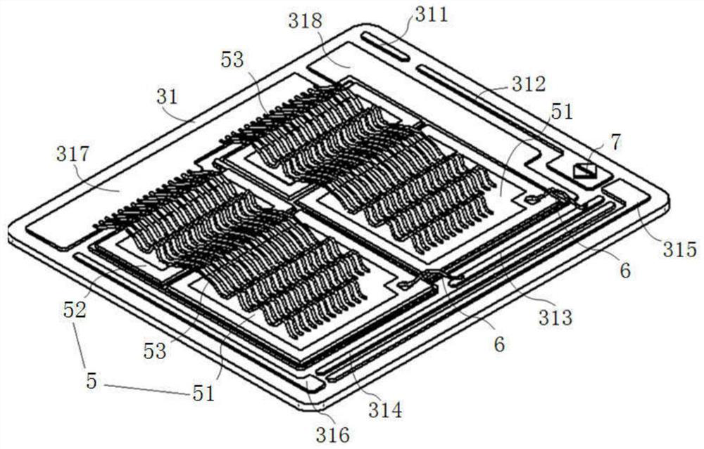
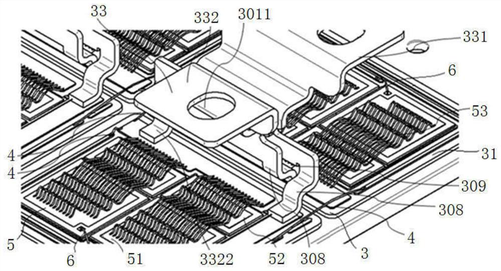
[0031] Such as Figure 1~3 As shown, the power semiconductor module packaging structure proposed by the present invention includes a substrate 1; a housing 2, which is sealed and fastened to the substrate 1; In the accommodation space, it is used to form a topology control circuit structure. The power semiconductor module subunit 3 includes a plurality of backing boards 31 arranged at intervals on the substr...
PUM
 Abstract
Description
Claims
Application Information