Method for welding components on circuit board

A circuit board and component technology, applied in the field of circuit board welding components, can solve the problems of cumbersome manual welding operation, low production efficiency, circuit board damage, etc.

Active Publication Date: 2019-11-01
台州市艾赛康电子有限公司
View PDF5 Cites 2 Cited by
  • Summary
  • Abstract
  • Description
  • Claims
  • Application Information

AI Technical Summary

Problems solved by technology

[0005] The form of wave soldering is limited to tinning the lower surface of the circuit board. During the process of tinning, if the tin liquid directly contacts the SMD components, the high temperature will re-melt the joints between the SMD components and the circuit board. Soldering will cause damage to the circuit board, so the wave soldering method can only solder the plug-in, and can only solder the circuit board where the patch component and the plug-in component are on the same side, so the application of wave soldering is extremely limited. If you want to complete the processing of this kind of circuit board, you must manually carry out the welding operation, and the manual welding operation is cumbersome and the production efficiency is low.

Method used


Image

  • Method for welding components on circuit board
  • Method for welding components on circuit board
  • Method for welding components on circuit board

Examples


Embodiment Construction

[0046] The present invention will be described in further detail below in conjunction with the accompanying drawings.

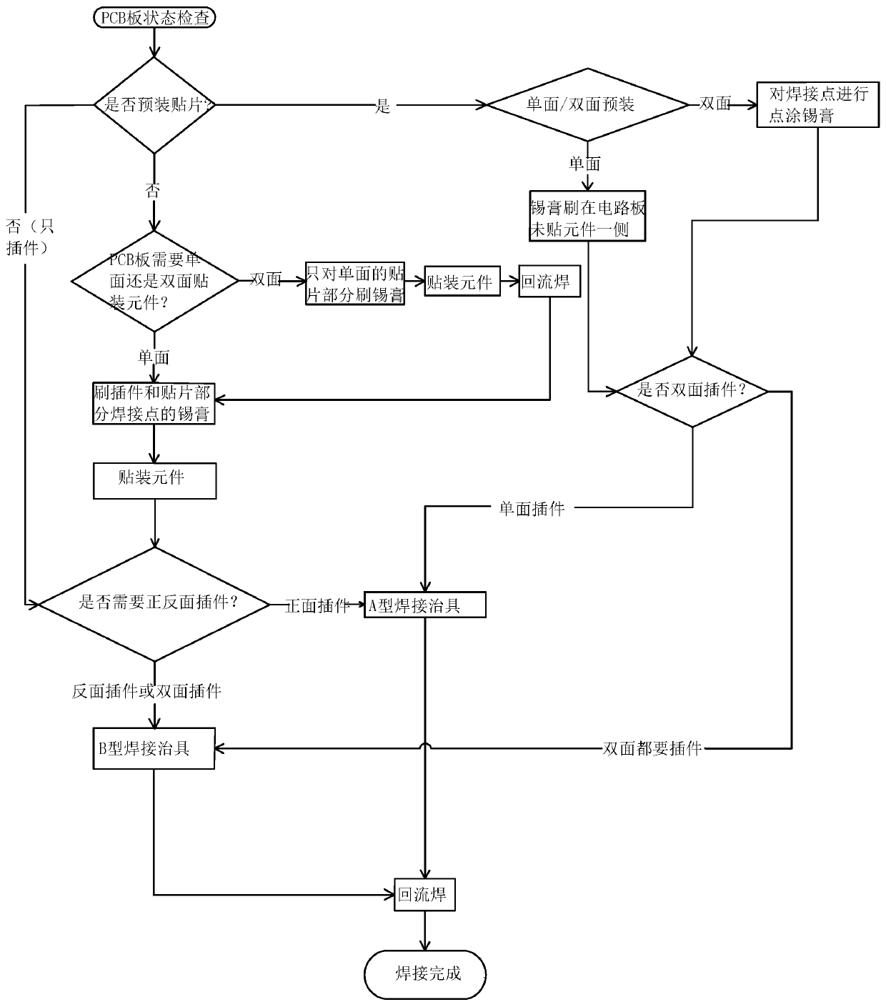
[0047] like figure 1 As shown, a method for soldering components on a circuit board mainly includes the following steps:

[0048] S1 PCB copper-clad circuit boards are divided into two types according to the factory specifications: pre-installed boards with pre-installed patches and empty boards without any components. The processes used for pre-installed boards and empty boards are different. , so the circuit board needs to be classified first after entering the factory. The classification is based on whether the circuit board has been pre-installed with patches. If there is pre-installation, it is pre-installed on one side or double-sided. Whether double-sided chips are needed, and whether double-sided plug-ins are needed, after specific subdivision, the mainstream circuit boards that are widely used at present mainly include the following types:

[0049]...


PUM


Abstract

The invention discloses a method for welding components on a circuit board, and relates to the circuit board production process. The method is used for solving the problems of narrow wave soldering application range and low production efficiency. The method comprises the following steps of brushing tin, namely brushing solder paste on patches and plug-in parts on the circuit board; SMD componentsor inserting components, namely installing SMD components or inserting components onto the circuit board; placing a die and positioning, bearing the circuit board with the components by using a welding jig so as to keep the circuit board in a horizontal state; carrying out heating welding, and carrying out reflow soldering on the welding jig provided with the circuit board; detecting and packaging: inspecting the welded circuit board, and packaging and storing the circuit board after ensuring that welding spots are in sufficient contact and are full. Compared with the prior art, by adopting the method, SMD components and inserting components can be mounted on the circuit board at the same time and welded synchronously. A large number of processing steps can be reduced compared with a wavesoldering mode. The manual participation degree is reduced. Therefore, the production efficiency of the circuit board can be greatly improved.

Description

technical field [0001] The invention relates to a circuit board production process, in particular to a method for welding components on a circuit board. Background technique [0002] The circuit board is the carrier of electronic components and the connection provider between electronic components. In all fields involving electronic circuits, basically all need to be applied to circuit boards. According to different types, circuit boards can be divided into covering Copper plate, aluminum substrate, ceramic circuit board, etc. [0003] At present, the Chinese invention patent with the authorized notification number CN106413282B discloses a partial wave soldering process for electronic circuit boards, which includes the following steps, providing an electronic circuit board to be soldered whose soldering surface is divided into a surface mount device area and a plug-in area; The soldered electronic circuit board is sent into the device coated with flux, and the spraying rang...

Claims


Application Information

Patent Timeline
Patent Type & Authority Applications(China)
IPC IPC(8): H05K3/34
CPCH05K3/341H05K3/3447H05K3/3494
Inventor 吴作金
Owner 台州市艾赛康电子有限公司
Why Eureka
Try Eureka