Supercharge Your Innovation With Domain-Expert AI Agents!

Full-automatic wafer probe station and full-automatic wafer testing device

A wafer test, fully automatic technology, applied in the semiconductor field, to achieve the effect of ensuring motion stability and precision

Inactive Publication Date: 2019-11-05
深圳市森美协尔科技有限公司
View PDF7 Cites 0 Cited by
  • Summary
  • Abstract
  • Description
  • Claims
  • Application Information

AI Technical Summary

Problems solved by technology

Therefore, the traditional manual probe test bench and semi-automatic probe test bench can no longer meet the requirements, replaced by a high-speed, high-precision, high-automation, high-reliability fully automatic wafer probe test bench

Method used


Image

  • Full-automatic wafer probe station and full-automatic wafer testing device
  • Full-automatic wafer probe station and full-automatic wafer testing device
  • Full-automatic wafer probe station and full-automatic wafer testing device

Examples


Embodiment Construction

[0026] The specific implementation manners of the present invention will be further described in detail below in conjunction with the accompanying drawings and embodiments. The following examples are used to illustrate the present invention, but are not intended to limit the scope of the present invention.

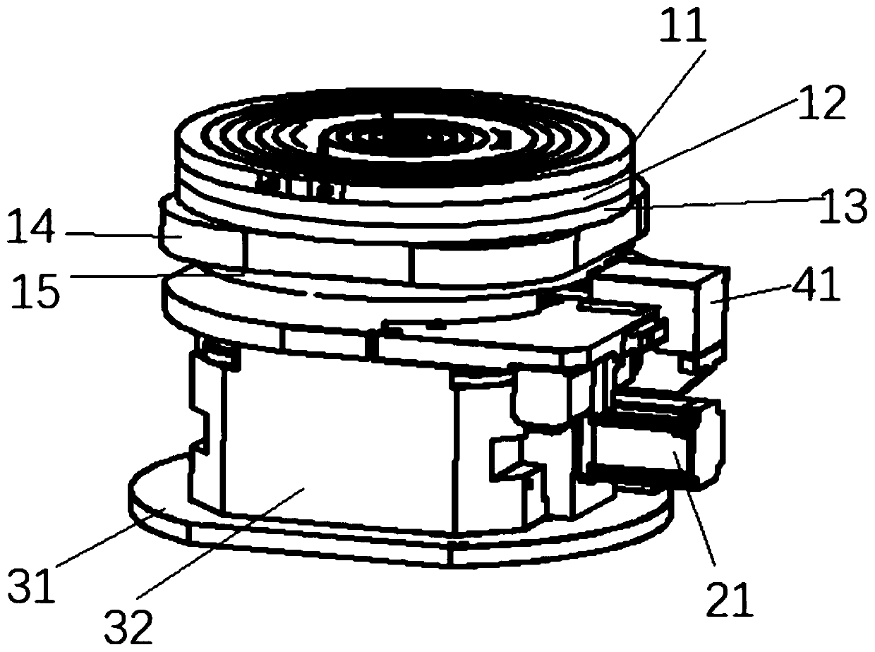
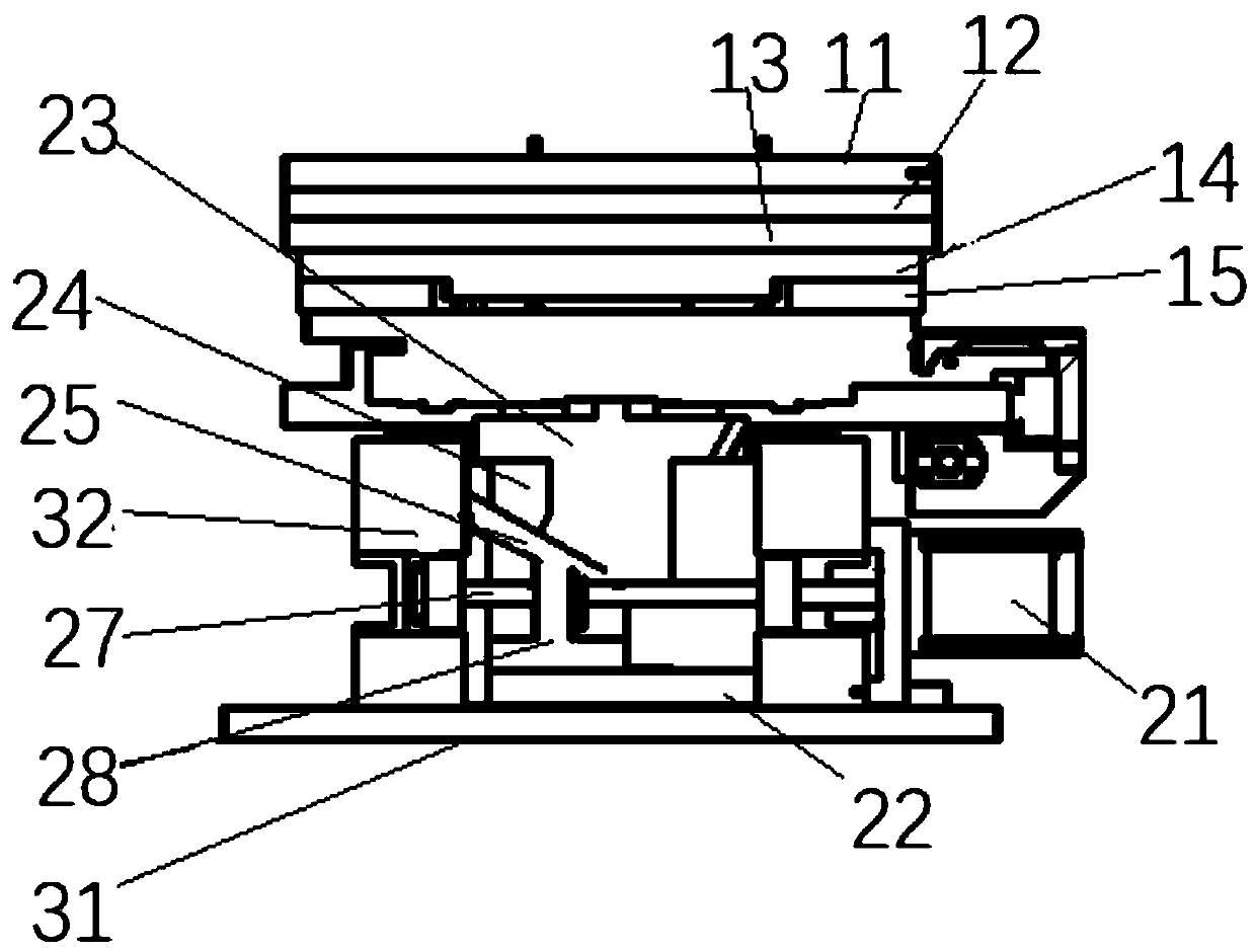
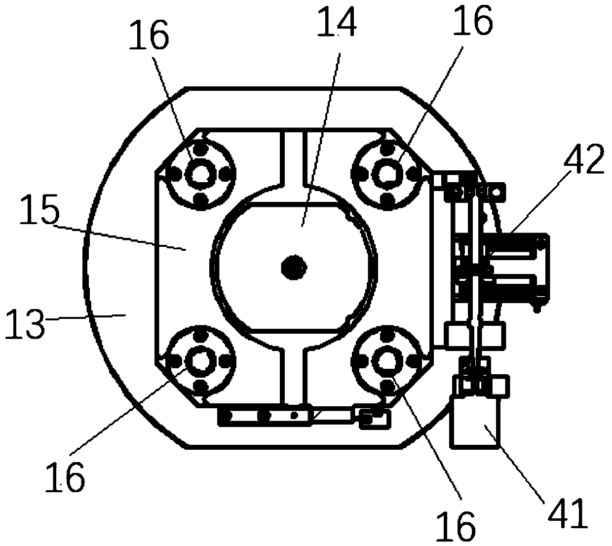
[0027] Such as Figure 1-3 As shown, in this embodiment, the fully automatic wafer probe station used for wafer testing includes a wafer stage, a rotary motion part located under the wafer stage, a vertical motion part located under the rotary motion part, and a vertical The casting base 31 at the bottom of the moving part and the body seat 32 formed by extending upward from the base 31 . The quality of each component increases sequentially from top to bottom to form a stable structure.

[0028] In this embodiment, the fully automatic wafer probe station can control the vertical movement of the wafer to be tested along the Z axis through the vertical movement part and co...


PUM


Abstract

The invention relates to a full-automatic wafer probe station for wafer testing. The full-automatic wafer probe station comprises a bearing table, a vertical moving component located below the bearingtable and a fixed base located at the bottom of the vertical moving component. The bearing table comprises a bottom plate, a plurality of base plates stacked on the upper surface of the bottom plateand a positioning part fixed to the bottom plate, and the positioning part is used for controlling the bearing table to move vertically along a fixed axis. According to the full-automatic wafer probestation for wafer testing in the invention, the motion stability and precision in the wafer testing process are ensured through a multi-reinforced stable structure.

Description

technical field [0001] The invention relates to the technical field of semiconductors, in particular to a fully automatic wafer probe station and fully automatic wafer testing equipment. Background technique [0002] Wafer testing is an important part of the chip manufacturing industry and one of the main statistical methods for chip yield. As the diameter and density of wafers gradually increase, the difficulty and cost of wafer testing become higher and higher, which also makes the chip require longer testing time and more sophisticated mechanical devices and computer systems to perform testing. Work and monitor test results. The most basic point of wafer testing is: wafer testing must be able to identify good or bad chips, and make qualified chips continue to enter the following packaging process. In order to ensure effective testing of chip functions and yields, packaging manufacturers and equipment manufacturers need to continue to explore, and then find high-precisio...

Claims


Application Information

Patent Timeline
IPC IPC(8): G01R31/26G01R1/02G01R1/04G01R1/067
CPCG01R1/02G01R1/04G01R1/06705G01R31/2601
Inventor 刘世文江有清
Owner 深圳市森美协尔科技有限公司
Features
  • R&D
  • Intellectual Property
  • Life Sciences
  • Materials
  • Tech Scout
  • Unparalleled Data Quality
  • Higher Quality Content
  • 60% Fewer Hallucinations
Learn More