An integrated circuit with ultra-low offset voltage based on bipolar process

A technology of offset voltage and bipolar technology, which is applied in the direction of adjusting electrical variables, control/regulation systems, instruments, etc., and can solve the problems of no ultra-low offset voltage.

Active Publication Date: 2021-09-21
GUIZHOU ZHENHUA FENGGUANG SEMICON
View PDF6 Cites 0 Cited by
  • Summary
  • Abstract
  • Description
  • Claims
  • Application Information

AI Technical Summary

Problems solved by technology

However, so far, there is no application for ultra-low offset voltage using the technical solution described in the present invention.

Method used


Image

  • An integrated circuit with ultra-low offset voltage based on bipolar process
  • An integrated circuit with ultra-low offset voltage based on bipolar process
  • An integrated circuit with ultra-low offset voltage based on bipolar process

Examples


specific Embodiment approach

[0073] The specific embodiment of the method of the present invention is as follows:

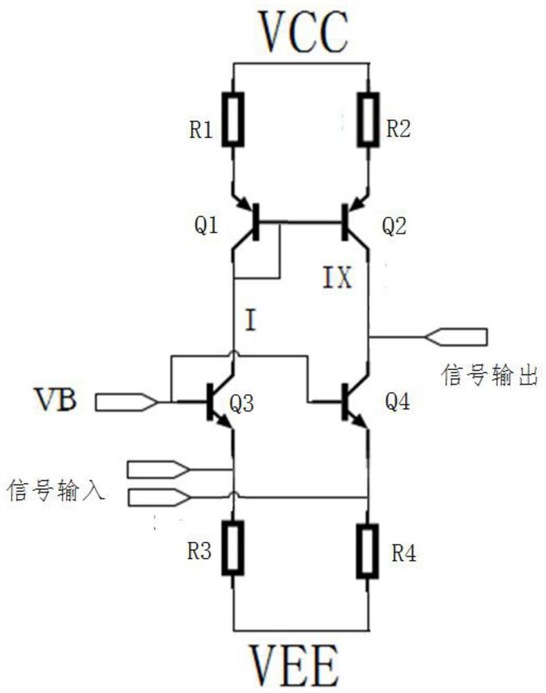
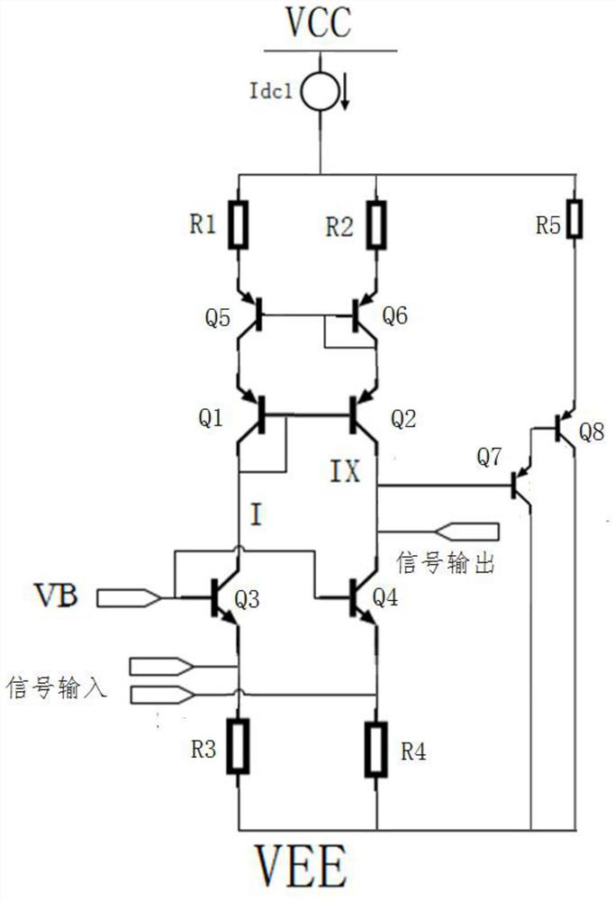
[0074] In order to eliminate the system disorders generated by the existing dual-transduction single circuit, the double transfers matching technology is used to implement signal dual transfers, such as attaching image 3 . Q1, Q2, Q5, Q6, Q7, Q8 are the same type of PNP tube, resistance R1, R2, R5 resistance ratio is R1 = R2 = 2r5 = R, set the appropriate bias voltage, make NPN tube Q3, Q4 collector electrode Current is i 1 , Set constant current power IDC1 current to 4i 1 . Set Q1, Q2, Q5, Q6, Q7, Q8 magnification is β 1 . At this time, the current error is IX 1 :

[0075]

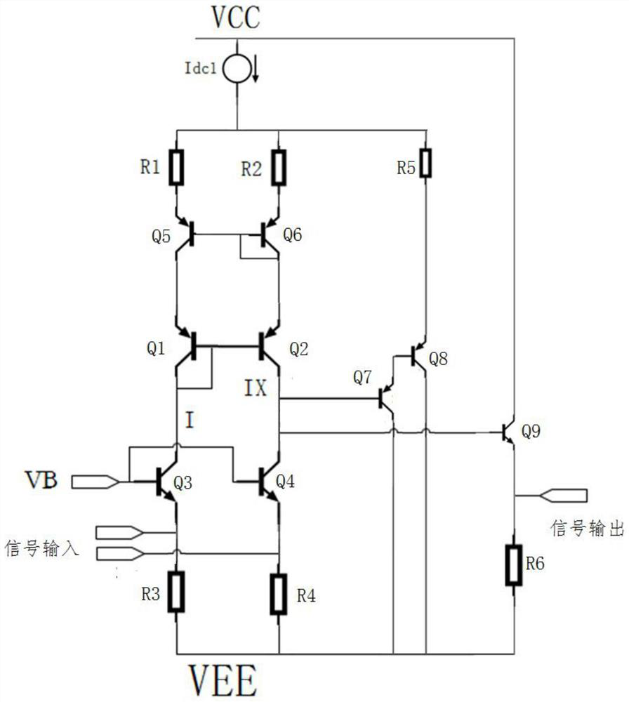
[0076] In order to eliminate the effect of Q9 base current on the matching of the circuit, Figure 4 The circuit shown is compensated for the Q9 tube base current. However, at this time, Q9 is inconsistent with the Q10 base current. Set up NPN tube Q9, Q10, Q11 current amplification is β 2 , Set Q9 emitter current to i 2 ,...


PUM


Abstract

An integrated circuit with ultra-low offset voltage based on a bipolar process discloses a method for solving the system offset problem of a dual-input-to-single-output integrated circuit in a bipolar process. The method adopts the double-rotation single-matching technology, combines the base current compensation technology and the current load compensation technology, and reduces the influence of the base current of the bipolar device on the system imbalance. The output terminal of the double-rotation single matching circuit is connected to the base current compensation circuit; the base current compensation circuit is connected to the double-rotation single matching circuit; the current load compensation circuit is connected to the double-rotation single matching circuit, the base current compensation circuit circuit connected. The advantages of this circuit: (1) reduce the influence of the base current of the bipolar transistor on the imbalance of the circuit system, and improve the circuit matching precision; (2) improve the circuit gain; (3) the current matching is not affected by the large current output. The invention is widely used in precision operational amplifiers based on bipolar technology, low offset comparators, high-precision AD / DA converters and other related fields.

Description

Technical field [0001] The present invention relates to a semiconductor integrated circuit, and more particularly to a bipolar semiconductor integrated circuit, in particular, to a bipolar ultra-low offset voltage integrated circuit. Background technique [0002] For the integrated circuit output from the dual input single output, the offset voltage is an important design parameter, and when the bipolar process is used to design the integrated circuit design, for figure 1 The dual input single output dual-input single output dual rotation unit circuit diagram, in which the bias voltage is set to the NPN tube Q3 collector current is I, and the NPN tube Q4 collector current is I, and the PNP tube Q1 is set. Q2 current amplification is β 1 , The PNP tube Q2 collector current is An imbalance current Therefore, since there is a certain inherent base current in which the bipolar device exists, the integrated circuit output of the dual input single output has an inherent system disord...

Claims


Application Information

Patent Timeline
Patent Type & Authority Patents(China)
IPC IPC(8): G05F1/56
CPCG05F1/56
Inventor 唐毓尚代松袁兴林蒋冰桃贾要水
Owner GUIZHOU ZHENHUA FENGGUANG SEMICON
Why Eureka
Try Eureka