Bipolar process-based integrated circuit with ultralow offset voltage

An offset voltage, integrated circuit technology, applied in the direction of adjusting electrical variables, control/regulating systems, instruments, etc., can solve problems such as ultra-low offset voltage

Active Publication Date: 2019-11-05
GUIZHOU ZHENHUA FENGGUANG SEMICON
View PDF6 Cites 0 Cited by
  • Summary
  • Abstract
  • Description
  • Claims
  • Application Information

AI Technical Summary

Problems solved by technology

However, so far, there is no application for ultra-low offset volta

Method used


Image

  • Bipolar process-based integrated circuit with ultralow offset voltage
  • Bipolar process-based integrated circuit with ultralow offset voltage
  • Bipolar process-based integrated circuit with ultralow offset voltage

Examples


specific Embodiment approach

[0073] The specific implementation of the inventive method is as follows:

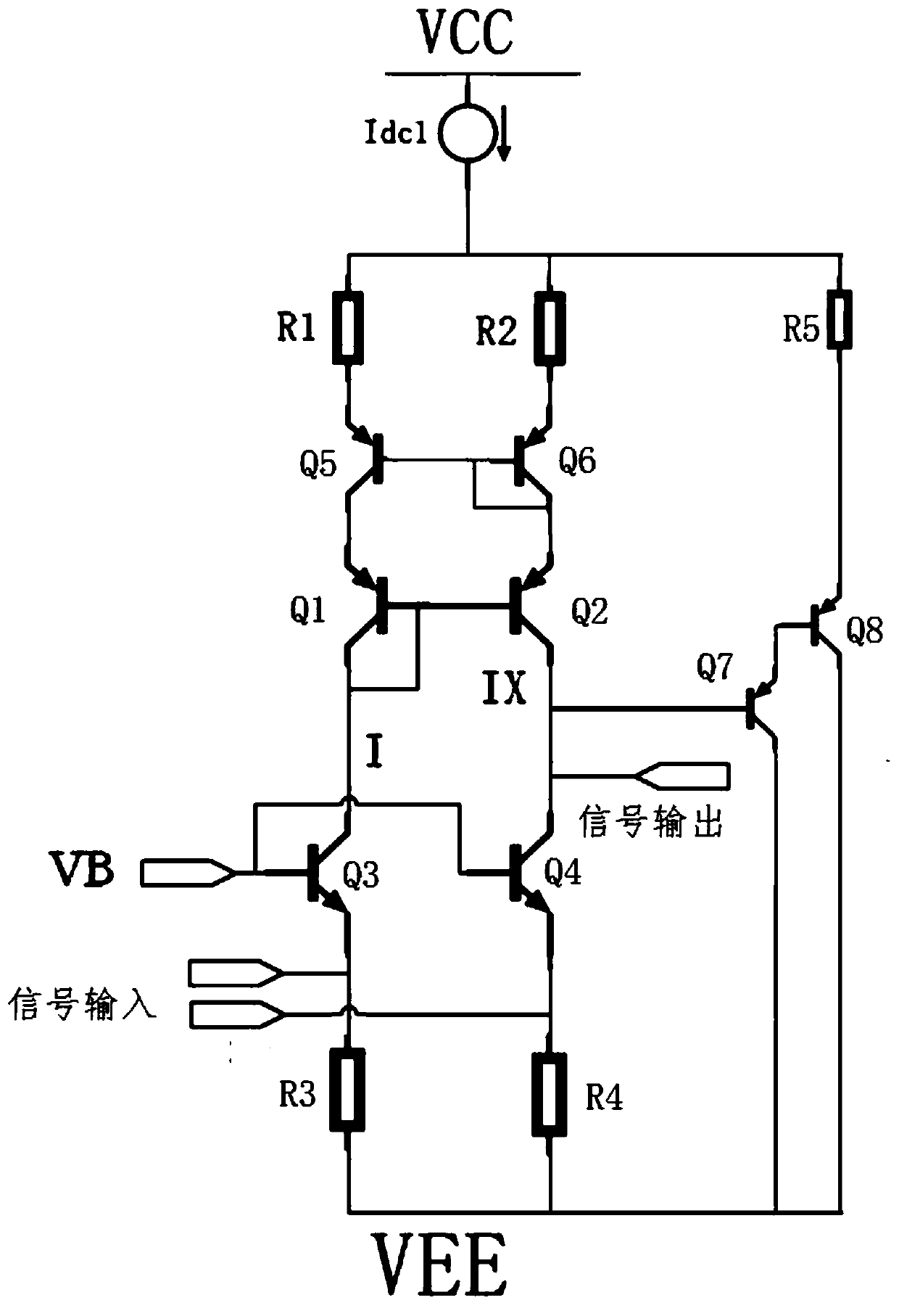
[0074] In order to eliminate the system imbalance caused by the existing double-to-single circuit, the double-to-single matching technology is used to realize the signal double-to-single, as attached image 3 . Q1, Q2, Q5, Q6, Q7, and Q8 are PNP tubes of the same type. The resistance ratio of resistors R1, R2, and R5 is R1=R2=2R5=R. Set an appropriate bias voltage to make the collectors of NPN tubes Q3 and Q4 current is I 1 , set the constant current power supply Idc1 current to 4I 1 . Set the amplification factor of Q1, Q2, Q5, Q6, Q7, Q8 as β 1 . At this time the current error is IX 1 :

[0075]

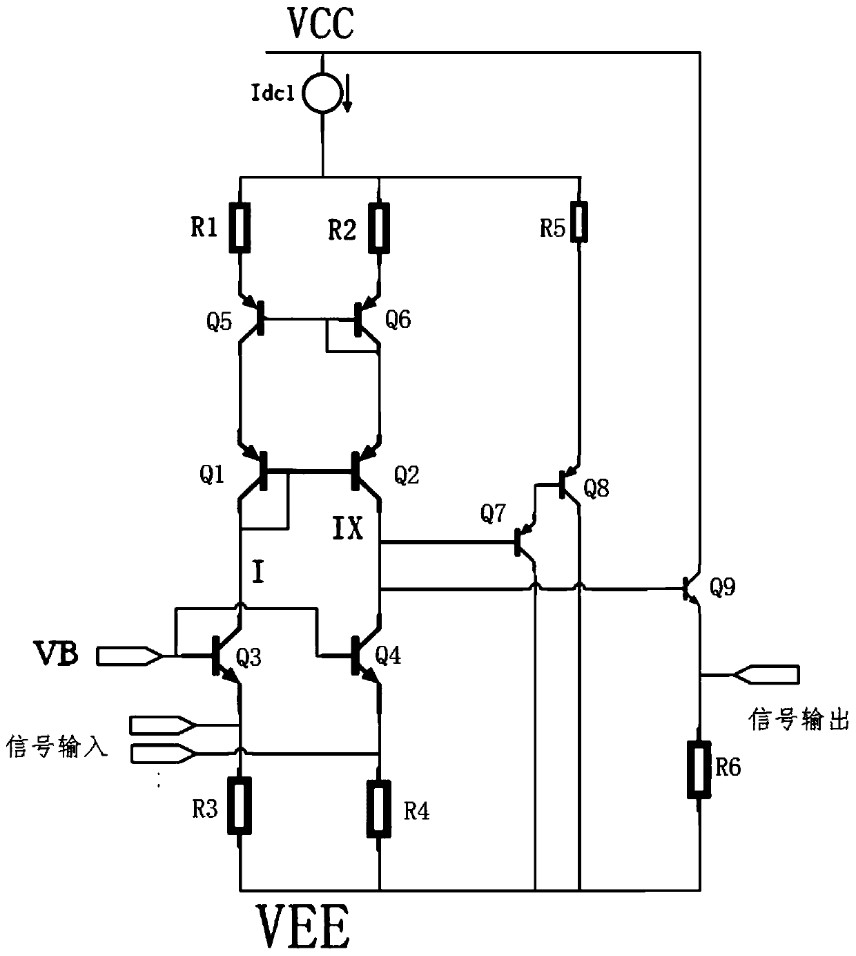
[0076] In order to eliminate the influence of the base current of Q9 on the circuit matching, it is adopted as Figure 4 The circuit shown compensates the base current of the Q9 tube. But at this time, the base currents of Q9 and Q10 are inconsistent. Set the current amplification factor of NPN...


PUM


Abstract

The invention discloses a bipolar process-based integrated circuit with an ultralow offset voltage. With the method of the invention adopted, the offset problem of a bipolar process-based double-input-to-single-output conversion integrated circuit system can be solved. According to the integrated circuit of the invention, a double-input-to-single-output conversion matching technology is adopted; and a base current compensation technology and a current load compensation technology are combined; and therefore, the influence of the base current of a bipolar device on system offset is reduced. Theoutput end of a double-input-to-single-output conversion matching circuit is connected with a base current compensation circuit; the base current compensation circuit is connected with the double-input-to-single-output conversion matching circuit; and a current load compensation circuit is connected with the double-input-to-single-output conversion matching circuit and the base current compensation circuit. With the integrated circuit of the invention adopted, the influence of the base current of a bipolar transistor on the offset of the circuit system is reduced, and the matching precision of the circuit is improved; the gain of the circuit is improved; and current matching is not affected by large current output. The integrated circuit is widely applied to bipolar process-based preciseoperational amplifiers, low-offset comparators and high-precision AD/DA devices and other related fields.

Description

technical field [0001] The present invention relates to a semiconductor integrated circuit, more specifically, to a bipolar semiconductor integrated circuit, specifically, to a bipolar ultra-low offset voltage integrated circuit. Background technique [0002] For integrated circuits with dual input and single output, offset voltage is an important design parameter. When using bipolar technology for integrated circuit design, for example figure 1 The double-input single-output double-turn single-unit circuit diagram of the shown bipolar process, in this circuit, set the bias voltage so that the collector current of the NPN tube Q3 is I, and the collector current of the NPN tube Q4 is I, and the PNP tubes Q1, Q2 current magnification is β 1 , then the collector current of PNP tube Q2 is produces an offset current Therefore, due to the inherent base current of the bipolar device, the dual-input and single-output integrated circuit has an inherent system imbalance, and the ...

Claims


Application Information

Patent Timeline
IPC IPC(8): G05F1/56
CPCG05F1/56
Inventor 唐毓尚代松袁兴林蒋冰桃贾要水
Owner GUIZHOU ZHENHUA FENGGUANG SEMICON
Why Eureka
Try Eureka