Image sensor and method for forming image sensor

An image sensor and patterning technology, applied in the direction of electric solid-state devices, semiconductor devices, electrical components, etc., can solve the problems of reducing manufacturing time and manufacturing costs, improve reliability, reduce the possibility of residues, and reduce process steps cost effect

Inactive Publication Date: 2019-11-05
HUAIAN IMAGING DEVICE MFGR CORP
View PDF4 Cites 0 Cited by
  • Summary
  • Abstract
  • Description
  • Claims
  • Application Information

AI Technical Summary

Problems solved by technology

[0004] However, the existing image sensor needs to reduce the manufacturing time and manufacturing cost, and the reliability of the existing image sensor needs to be improved

Method used


Image

  • Image sensor and method for forming image sensor
  • Image sensor and method for forming image sensor
  • Image sensor and method for forming image sensor

Examples


Embodiment Construction

[0032] As described in the background, there is a need to reduce manufacturing time and cost of existing image sensors, and to improve reliability of existing image sensors.

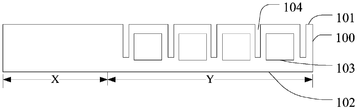
[0033] Figure 1 to Figure 6 It is a schematic cross-sectional structure diagram of an embodiment of the forming process of an image sensor.

[0034] Please refer to figure 1 , provide a substrate 100, the substrate 100 has an opposite first surface 101 and a second surface 102, the substrate 100 includes a region X and a region Y, the substrate 100 of the region Y has several photoelectric doping region 103 and a trench 104 surrounding the optoelectronic doped region 103 .

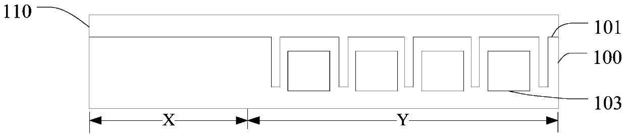
[0035] Please refer to figure 2 , filling the trench 104 to form an isolation structure (not shown); while forming the isolation structure, an initial anti-reflection layer 110 is formed on the surface of the first surface 101 .

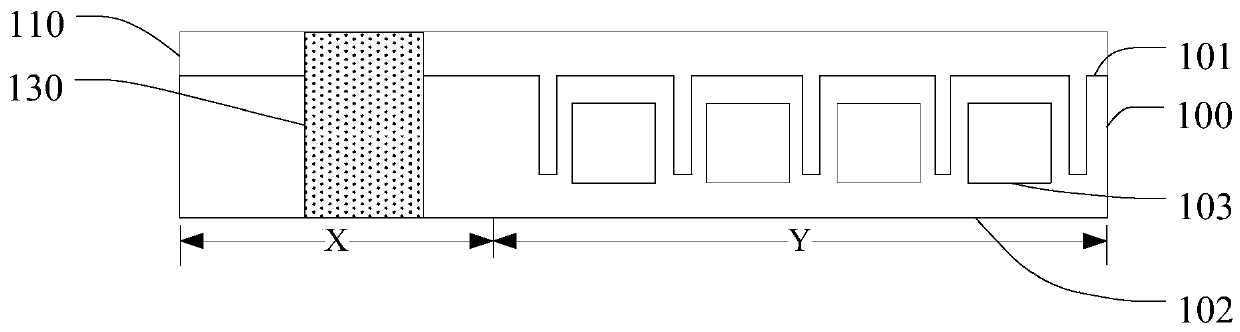
[0036] Please refer to image 3 , forming a conductive plug 130 penetrating through the substrate...


PUM


Abstract

The invention provides an image sensor and a method for forming the image sensor. The image sensor comprises a step of providing a first substrate with a first surface, a step of forming an anti-reflection layer on the first surface of the first substrate, wherein the thickness of the anti-reflection layer is a predetermined thickness in a direction perpendicular to the first surface, a step of forming an through hole which passes through the anti-reflection layer and the first substrate, a step of forming a first conductive layer in the through hole, wherein the anti-reflection layer exposesa surface of the first conductive layer, and a step of forming a grid layer on a surface of the anti-reflection layer after forming the first conductive layer. According to the method, the time and cost in manufacturing the image sensor can be saved.

Description

technical field [0001] The invention relates to the field of semiconductor manufacturing, in particular to an image sensor and a forming method thereof. Background technique [0002] An image sensor refers to a device that converts optical signals into electrical signals. Generally, large-scale commercial image sensor chips include charge-coupled device (CCD) and complementary metal-oxide semiconductor (CMOS) image sensor chips. Compared with traditional CCD sensors, CMOS image sensors have the characteristics of low power consumption, low cost and compatibility with CMOS technology, so they are more and more widely used. The pixel unit of the CMOS image sensor is the core device for the image sensor to realize light sensing. The most commonly used pixel cell is an active pixel structure consisting of a photodiode and multiple transistors. In these devices, the photodiode is the photosensitive unit, which realizes the collection and photoelectric conversion of light, and t...

Claims


Application Information

Patent Timeline
Patent Type & Authority Applications(China)
IPC IPC(8): H01L27/146
CPCH01L27/1462H01L27/1464H01L27/14643H01L27/14685H01L27/14689
Inventor 王东金子貴昭
Owner HUAIAN IMAGING DEVICE MFGR CORP
Why Eureka
Try Eureka