LED display screen module adopting stacking according to blocks for realizing packaging, and packaging method

A technology of LED display screen and LED chip, which is applied in the direction of identification devices, instruments, etc., can solve the problems of large pixel pitch, low display resolution, and insufficient display effect, and achieve high resolution, low labor cost, and high display effect. Better delicate effect

Pending Publication Date: 2019-11-08
SHENZHEN JIEJIANDA INNOVATION TECH CO LTD
View PDF0 Cites 2 Cited by
  • Summary
  • Abstract
  • Description
  • Claims
  • Application Information

AI Technical Summary

Problems solved by technology

[0003] The technical problem to be solved by the present invention is to provide a LED display module and packaging method that are stacked and packaged by blocks, which overcomes the excessively large pixel pitch caused by the packaging process of the LED display in the prior art, the relatively low display resolution, and the poor display effect. Defects that are not detailed enough

Method used


Image

  • LED display screen module adopting stacking according to blocks for realizing packaging, and packaging method
  • LED display screen module adopting stacking according to blocks for realizing packaging, and packaging method
  • LED display screen module adopting stacking according to blocks for realizing packaging, and packaging method

Examples


Embodiment Construction

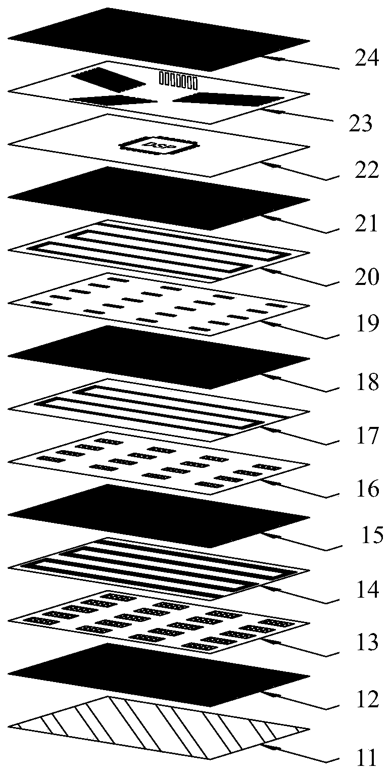
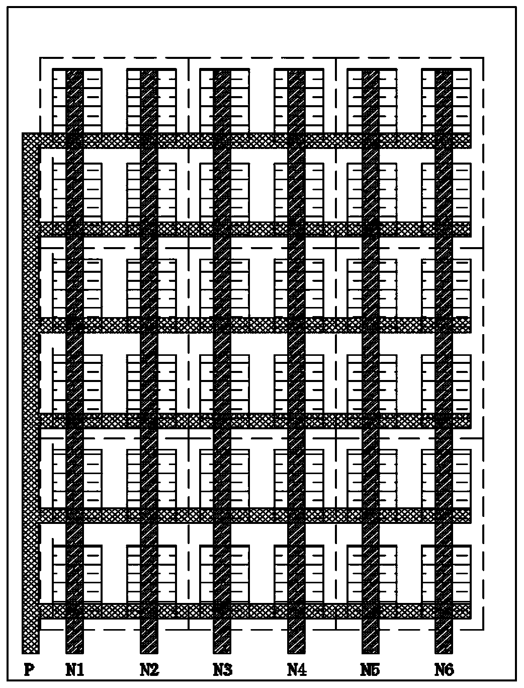
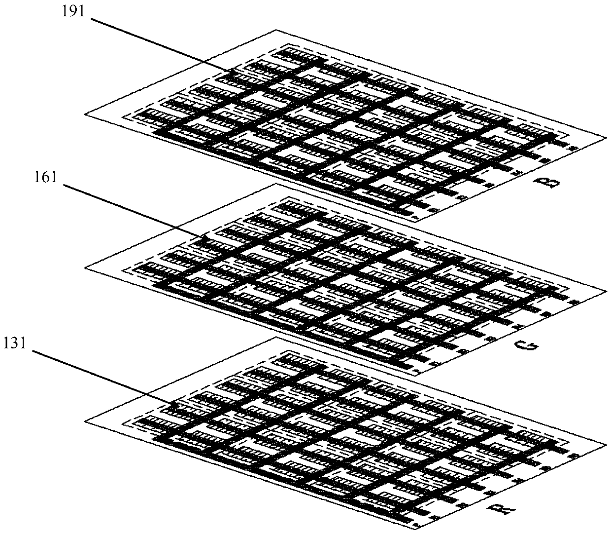
[0026] Such as figure 1 , figure 2 , image 3 As shown, the LED display module of the present invention stacked and packaged by blocks includes a light-transmitting screen substrate 11 on the surface of the display screen, and a red LED layer 13 and a green LED layer 13 are stacked in any order on the light-transmitting screen substrate 11. Layer 16, blue LED layer 19, and LED light emission control device layer 22 located on red LED layer 13, green LED layer 16, and blue LED layer 19. The green LED layer 16 is composed of a green LED chip block 161 which can be transferred as a whole, and the blue LED layer 19 is composed of a blue LED chip block 191 which can be transferred and placed as a whole. The translucent screen The substrate 11, the red LED layer 13, the green LED layer 16, the blue LED layer 19, and the LED lighting control device layer 22 pass through the shadowless adhesive layer 12, the shadowless adhesive layer 15, the shadowless adhesive layer 18, and the sh...


PUM


Abstract

The invention discloses an LED display screen module adopting stacking according to blocks for realizing packaging, and a packaging method. The LED display screen module comprises a light-pervious screen base plate on the surface of a display screen, a red-light LED layer, a green-light LED layer, a blue-light LED layer, as well as LED light-emitting control device layers on the red-light LED layer, the green-light LED layer and the blue-light LED layer are sequentially stacked on the light-pervious screen base plate according to any sequence, the red-light LED layer is composed of a red-lightLED chip group block capable of being integrally transferred and placed, the green-light LED layer is composed of a green-light LED chip group block capable of being integrally transferred and placed, and the blue-light LED layer is composed of a blue-light LED chip group block capable of being integrally transferred and placed.

Description

technical field [0001] The invention relates to the technical field of chip packaging, in particular to an LED display module and a packaging method that are stacked and packaged by blocks. Background technique [0002] The LED color screen has the advantages of fast response, high power saving and light output efficiency, and active light emission. In particular, it can realize the effects of virtual reality such as AR and VR, which will be the main force for future display integration. However, at this stage, MiNi LED or MiCRO LED are limited by wire bonding or flip-chip technology, and are limited in terms of pixels. Now it can achieve about P0.8, that is, the distance between each center point is 0.8mm. In the prior art, when manufacturing LED display modules, independent single LED chips are absorbed and then transferred as a whole (massive transfer), so how to make the pitch of the LED chips arranged on the LED display module smaller and how to Die bonding with small...

Claims


Application Information

Patent Timeline
Patent Type & Authority Applications(China)
IPC IPC(8): G09F9/33
CPCG09F9/33
Inventor 涂波郑香奕
Owner SHENZHEN JIEJIANDA INNOVATION TECH CO LTD
Why Eureka
Try Eureka