An array substrate and a display panel

A technology for display panels and array substrates, applied in semiconductor devices, electrical components, circuits, etc., can solve problems such as difficulty, and achieve the effect of increasing the aperture ratio, reducing the overall area, and increasing the pixel density.

Active Publication Date: 2021-10-15
YUNGU GUAN TECH CO LTD
View PDF0 Cites 0 Cited by
  • Summary
  • Abstract
  • Description
  • Claims
  • Application Information

AI Technical Summary

Problems solved by technology

However, it is still difficult to manufacture OLED display panels with relatively high pixel per inch (PPI)

Method used


Image

  • An array substrate and a display panel
  • An array substrate and a display panel
  • An array substrate and a display panel

Examples


Embodiment Construction

[0040] The present invention will be further described in detail below in conjunction with the accompanying drawings and embodiments. It should be understood that the specific embodiments described here are only used to explain the present invention, but not to limit the present invention. In addition, it should be noted that, for the convenience of description, only some structures related to the present invention are shown in the drawings but not all structures.

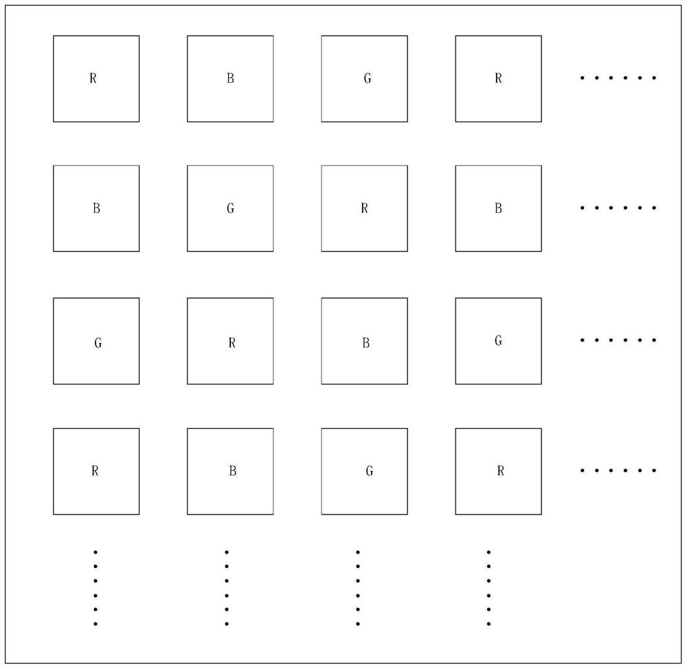
[0041] figure 1 It is a structural schematic diagram of an existing display panel. like figure 1 As shown, the display panel includes a red sub-pixel R, a green sub-pixel G and a blue sub-pixel B. The red sub-pixel R, the green sub-pixel G and the blue sub-pixel B are arranged on the display panel, and each sub-pixel has a certain opening area, so each sub-pixel occupies a certain area of ​​the display panel. The red sub-pixel R, green sub-pixel G and blue sub-pixel B form a pixel unit, and the area of ​​the di...


PUM

PropertyMeasurementUnit
thicknessaaaaaaaaaa

Abstract

The invention discloses an array substrate and a display panel. The array substrate includes a substrate; at least two groups of pixel circuit film layers, each group of pixel circuit film layers includes at least one pixel circuit; along the thickness direction of the substrate, at least two groups of pixel circuit film layers overlap. By arranging at least two sets of pixel circuit film layers on the substrate, along the thickness direction of the substrate, at least two sets of pixel circuit film layers overlap, thereby reducing the overall area of ​​the array substrate occupied by the pixel circuits, so that the array substrate can be arranged More pixel circuits are beneficial to increase the pixel arrangement density of the display panel and improve the PPI of the display panel.

Description

technical field [0001] Embodiments of the present invention relate to the field of display technologies, and in particular, to an array substrate and a display panel. Background technique [0002] Organic Light-Emitting Diode (OLED) display has become the current mainstream display technology due to its advantages of high contrast, high response speed, low power consumption, self-illumination and unique flexibility and bendability. [0003] In order to realize the independent control of the color of the display panel, the OLED display panel adopts the independent control of RGB three-color sub-pixels to achieve colorization. However, it is still difficult to manufacture an OLED display panel with a relatively high pixel per inch (PPI). Contents of the invention [0004] The invention provides an array substrate and a display panel to increase the pixel density of the display panel. [0005] In a first aspect, an embodiment of the present invention provides an array subst...

Claims


Application Information

Patent Timeline
Patent Type & Authority Patents(China)
IPC IPC(8): H01L27/32
CPCH10K59/131
Inventor 刘操朱平徐凯刘娜贾智信
Owner YUNGU GUAN TECH CO LTD
Why Eureka
Try Eureka