Probe for semiconductor probe test bench

A test bench and semiconductor technology, applied in electronic circuit testing, measuring electricity, measuring devices, etc., can solve the problems of poor welding quality of finished pins, difference in test results, affecting test results, etc., so as to reduce twisting force and prevent puncture. Wafers, the effect of improving accuracy

Active Publication Date: 2019-11-22
深圳市森美协尔科技有限公司
View PDF6 Cites 3 Cited by
  • Summary
  • Abstract
  • Description
  • Claims
  • Application Information

AI Technical Summary

Problems solved by technology

[0003] In the integrated circuit industry chain, integrated circuit testing is the only industry that runs through the entire process of integrated circuit production and application. If the integrated circuit design does not pass the prototype verification test, it can be put into mass production: in mass production, if the wafer fails to pass The mid-test of the probe test bench cannot be packaged in the next process; and the final test of the finished product after packaging is the final process of integrated circuit products. Only the circuits that pass the test can be shipped as formal integrated circuit products. Now The working principle of probes for semiconductors with probe test benches is as follows: during testing, the wafer is adsorbed on the carrier by a vacuum chuck and aligned with the probe electrical detector, and then the probes are in contact with each pad of the chip. Contact, under the drive of the power supply, the electrical tester looks at the circuit sideways and records the test results to judge whether the wafer is good or bad. On the same level, the wafer is subjected to a difference in position height during the test process. Some probes with lower positions can directly touch the wafer, while some probes with higher positions cannot touch the wafer, causing the wafer to be under test. , the test results are different, and some wafers cannot be tested. When the probe with a higher position touches the wafer, the probe with a lower position directly collides with the wafer, causing the probe tip to scratch the surface layer, causing the chip and the finished product after packaging Poor soldering quality of the pins can easily cause short circuit and affect the final test results. At the same time, the position is not on the same level. In addition, the operator adjusts the lifting speed of the loading table too fast, and the wafer directly hits the probe, causing the end of the probe to be damaged. Force bending, breaking, some probes crack directly, and after the wafer is stressed, the surface is directly scratched, further affecting the testing of the wafer, the measured results cannot be accurate, and affect the normal judgment of the wafer

Method used


Image

  • Probe for semiconductor probe test bench
  • Probe for semiconductor probe test bench
  • Probe for semiconductor probe test bench

Examples


Embodiment Construction

[0017] The following will clearly and completely describe the technical solutions in the embodiments of the present invention with reference to the accompanying drawings in the embodiments of the present invention. Obviously, the described embodiments are only some, not all, embodiments of the present invention. Based on the embodiments of the present invention, all other embodiments obtained by persons of ordinary skill in the art without making creative efforts belong to the protection scope of the present invention.

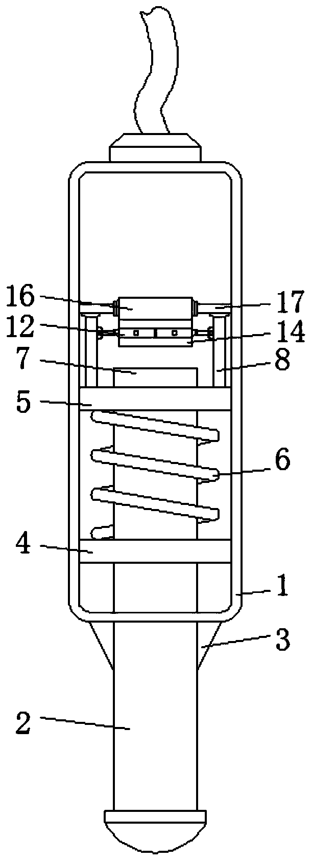
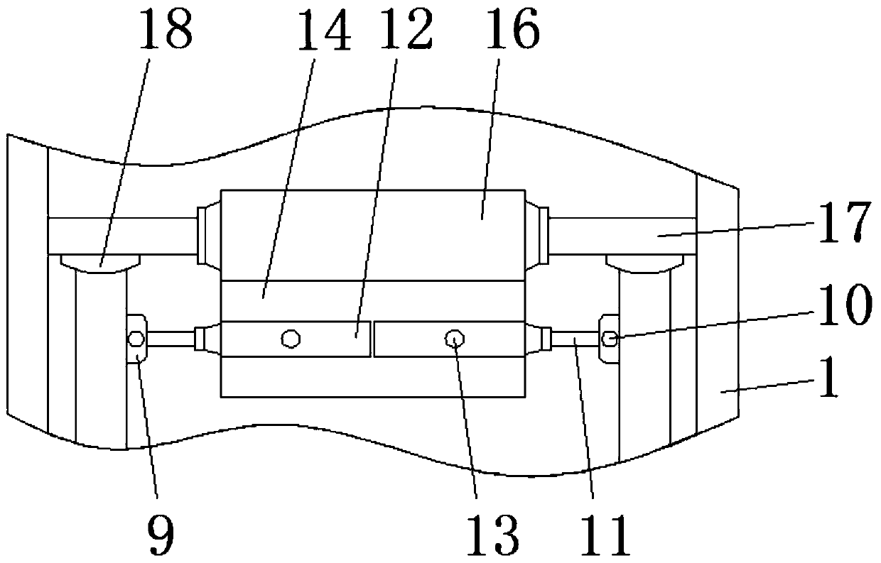
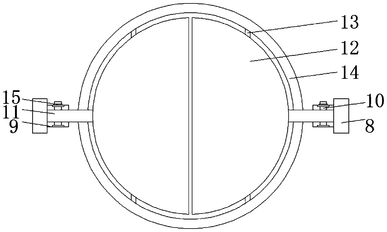
[0018] see Figure 1-3 , a probe for a semiconductor probe test bench, comprising a sleeve 1, a needle 2, the needle 2 is installed on the bottom of the sleeve 1, a positioning block 4 is fixedly installed inside the sleeve 1, and the inner wall of the positioning block 4 is connected to the The needle 2 is slidingly connected, so that the needle 2 can slide to different positions. The end of the needle 2 is fixedly connected with a sliding block 5 located ins...


PUM


Abstract

The invention, which relates to the technical field of integrated circuits, discloses a probe for a semiconductor probe test bench. The probe includes a casing tube and a needle. The needle is installed at the bottom of the casing tube; and a positioning block is fixedly installed inside the casing tube. A slidingblock arranged in the casing tube is fixedly connected to the end of the needle; anda spring is installed between the positioning block and the sliding block. When the needle is impacted by a bearing bench, the needle is contracted to the inner side instantaneously and thus the stateof the needle is optimized from hard contact to the elastic contact, so that the needle can adapt to the wafer position and thus the needle is contracted or expanded to different positions automatically in use. Besides, the needle can be in contact with different positions of the wafer; and when the needle is impacted, the needle is contracted automatically to reduce the impact force; with the elastic force effect, the twisting force of the needle is reduced; and thus the needle is in a a vertical state all the time during use. At the same time, the needle can be in contact with different positions of the wafer, thereby improving the accuracy of the wafer during testing.

Description

technical field [0001] The invention relates to the technical field of integrated circuits, in particular to a probe for a semiconductor probe test bench. Background technique [0002] The probe station is mainly used in the semiconductor industry, optoelectronic industry, integrated circuit and package testing. It is widely used in the research and development of precision electrical measurement of complex and high-speed devices, aiming to ensure quality and reliability, and reduce research and development time and device manufacturing process. cost. [0003] In the integrated circuit industry chain, integrated circuit testing is the only industry that runs through the entire process of integrated circuit production and application. If the integrated circuit design does not pass the prototype verification test, it can be put into mass production: in mass production, if the wafer fails to pass The mid-test of the probe test bench cannot be packaged in the next process; and ...

Claims


Application Information

Patent Timeline
Patent Type & Authority Applications(China)
IPC IPC(8): G01R31/28G01R1/067
CPCG01R1/06722G01R1/06794G01R31/2887
Inventor 施林荣
Owner 深圳市森美协尔科技有限公司
Why Eureka
Try Eureka