OLED pixel structure and display device

A technology of pixel structure and pixel unit, which is applied in the direction of static indicators, instruments, semiconductor devices, etc., can solve the problems of compensation errors, insufficient pixel layout space, etc., and achieve the effect of eliminating errors, reducing the difficulty of pixel layout, and avoiding compensation errors

Inactive Publication Date: 2019-11-22
KUNSHAN GO VISIONOX OPTO ELECTRONICS CO LTD
View PDF10 Cites 1 Cited by
  • Summary
  • Abstract
  • Description
  • Claims
  • Application Information

AI Technical Summary

Problems solved by technology

[0004] AMOLED products on the market generally use 7T1C pixel circuits, but in the process of compensating for threshold voltage drift, compensation errors will occur
Therefore, an 8T2C pixel circuit is proposed, but setting M8 will make the pixel layout space insufficient

Method used


Image

  • OLED pixel structure and display device
  • OLED pixel structure and display device
  • OLED pixel structure and display device

Examples


Embodiment Construction

[0025] The present invention will be described in detail below in conjunction with the accompanying drawings and embodiments.

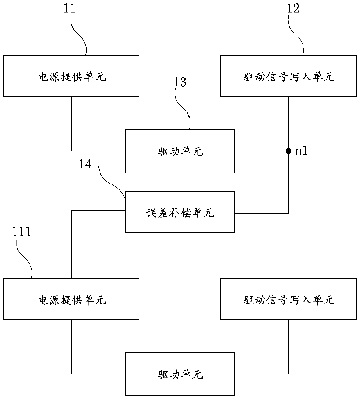
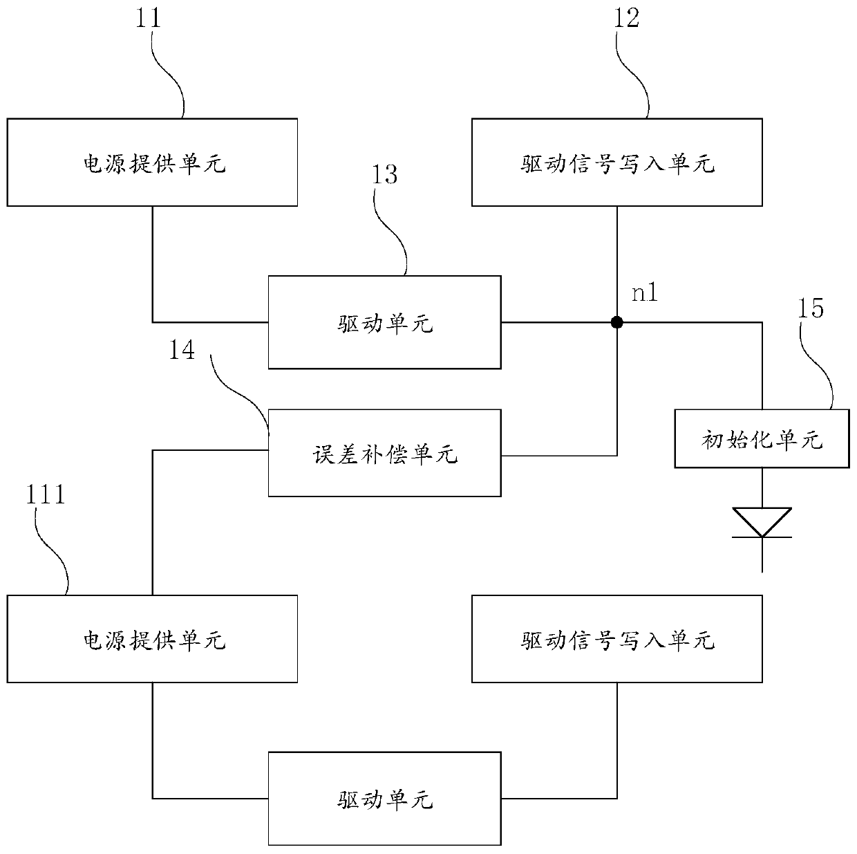
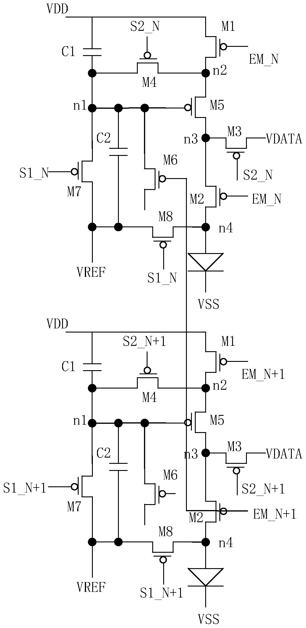
[0026] See figure 1 , is a structural schematic diagram of the first embodiment of the OLED pixel structure of the present invention. It includes a plurality of pixel units distributed in an array, wherein each pixel unit includes: a power supply unit 11 , a driving signal writing unit 12 , a driving unit 13 and an error compensation unit 14 .

[0027] Wherein, the driving unit 13 is connected to the power supply unit 11 and the driving signal writing unit 12, and the first node metal line at the first node n1 connected between the driving unit 13 and the driving signal writing unit 12 is connected to the next-level pixel unit The power supply unit 111 is used to form the error compensation unit 14 .

[0028] Specifically, the power supply unit 11 receives the light-emitting enable signal of the current stage, so as to provide the light-emitting dio...


PUM


Abstract

The invention provides an OLED pixel structure and a display device. The OLED pixel structure comprises a plurality of pixel units distributed in an array, and each pixel unit comprises a power supplyunit, a driving signal writing unit and a driving unit. The driving unit is connected with the driving signal writing unit and the power supply unit, stores a driving signal written by the driving signal writing unit, and generates a driving current matched with the driving signal by using a power supply signal provided by the power supply unit according to the driving signal so as to drive the light emitting diode. A first node metal wire of the driving unit, which is connected with the driving signal writing unit, is connected with a semiconductor layer of a next-stage pixel unit and is matched with a next-stage light-emitting enable signal wire of the next-stage pixel unit to form an error compensation unit. Therefore, an error of writing a driving signal by the driving signal writingunit is eliminated. In this way, compensation errors in the threshold voltage drift compensation process are avoided.

Description

technical field [0001] The invention relates to the field of display technology, in particular to an OLED pixel structure and a display device. Background technique [0002] In the manufacturing process of active (active) matrix organic light emitting diode (Active-matrix Organic Light Emitting Diode, AMOLED) circuit, due to the reasons of the process, there is usually a problem of uneven threshold voltage of TFT device parameters, which will cause AMOLED display The brightness is uneven during the process, and the display quality deteriorates. [0003] At present, the method adopted to solve the above-mentioned problems is through the internal pixel circuit or the compensation function of the external driver chip. But external drivers usually require additional chips, increasing the cost and complexity of the electronic system. Generally, the internal compensation of the pixel circuit only needs to use the pixel circuit with compensation function to realize the compensati...

Claims


Application Information

Patent Timeline
Patent Type & Authority Applications(China)
IPC IPC(8): G09G3/3233H01L27/32
CPCG09G3/3233H10K59/131
Inventor 周志伟宋艳芹李威龙张露韩珍珍胡思明
Owner KUNSHAN GO VISIONOX OPTO ELECTRONICS CO LTD
Why Eureka
Try Eureka