Glue coating crystal solidifying method and system thereof

A technology of solid crystal and glue covering, which is applied in the direction of electrical components, circuits, semiconductor devices, etc., can solve the problems of non-coincident position of crystal grain and glue point, difficulty in controlling the height of chip encapsulation, poor consistency of glue point size, etc., to achieve easy Finished product heat dissipation, reduce design layout and calculation difficulty, and ensure the effect of consistency

Inactive Publication Date: 2014-06-18
深圳翠涛自动化设备股份有限公司
View PDF2 Cites 7 Cited by
  • Summary
  • Abstract
  • Description
  • Claims
  • Application Information

AI Technical Summary

Problems solved by technology

[0009] In view of the above-mentioned deficiencies in the prior art, the object of the present invention is to provide a glue-coated die-bonding method and its system, aiming at solving the problem of misalignment of the crystal grain

Method used


Image

  • Glue coating crystal solidifying method and system thereof
  • Glue coating crystal solidifying method and system thereof

Examples


Example Embodiment

[0049] The present invention provides a glue-coated crystal solidification method and system thereof. In order to make the objectives, technical solutions, and effects of the present invention clearer and clearer, the present invention will be further described in detail with reference to the accompanying drawings and examples. It should be understood that the specific embodiments described here are only used to explain the present invention, but not to limit the present invention.

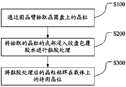
[0050] See figure 1 , figure 1 It is a flow chart of the method for coating and crystal fixing of the invention.

[0051] Such as figure 1 As shown, the glue-coating method for crystal fixing includes:

[0052] In step S100, the die on the wafer tray is picked up by the die attach arm.

[0053] Wherein, step S100 specifically includes:
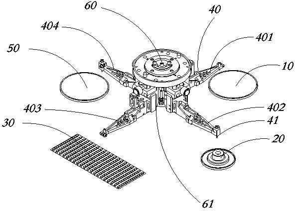
[0054] Step S110: align the center of the pick-up device at the end of the die attach arm and place it above the surface of the die on the wafer tray;

[0055] Step S120, l...


PUM


Abstract

The invention discloses a glue coating crystal solidifying method and a glue coating crystal solidifying system. The method comprises the following steps that A, crystal grains on a wafer disc are picked through a crystal solidifying arm; B, the bottoms of the picked crystal grains are immersed into a glue disc to be coated with glue water to be subjected to gluing treatment; C, the crystal grains subjected to the gluing treatment are bonded and welded on positions requiring crystal solidification on the carrier. One machine and control structure is adopted for crystal picking, and in addition, the glue taking is realized through wafers per se, so adverse phenomena that in the traditional mode, the blind points exist in bonding positions of the crystal grains and the glue points, the bonding surface distribution is nonuniform, the deviation of the crystal grains and the glue drip reset points is greater, the glue form is not full, the absorption firmness is poor, and the like can be avoided. The crystal solidifying method can be realized through adopting the independent system, the problem of collision when two independent mechanisms are used for production in the same station can be completely avoided, the mechanical structure is simplified, the control difficulty is reduced, and meanwhile, the product precision is also improved.

Description

technical field [0001] The invention relates to the field of semiconductor precision manufacturing and equipment, in particular to a glue-covered crystal-bonding method and system for IC and LED semiconductor packaging. Background technique [0002] The purpose of solid crystal is to fix the crystal grain (or chip) on the carrier, so that the input of thermal or electrical signal can be realized between the crystal grain (or chip) and the carrier. Whether the position of the grain (or chip) placed in the carrier package is accurate or not directly affects the luminous and conductive performance of the device. If the position of the grain (or chip) in the carrier package deviates, the light will not be fully emitted in the lighting device As a result, the brightness of the finished product will be affected, and in the integrated circuit, the electrical signal will not be fully connected, which will affect the efficacy of the finished product. Therefore, the precision of the ...

Claims


Application Information

Patent Timeline
IPC IPC(8): H01L33/00
CPCH01L33/62H01L2933/005H01L2933/0066
Inventor 孙亚雷米广辉罗尚峰
Owner 深圳翠涛自动化设备股份有限公司
Why Eureka
Try Eureka