A glue-covered crystal-bonding equipment

A technology of die bonding and equipment, which is applied in semiconductor/solid-state device manufacturing, electrical components, circuits, etc. It can solve problems such as the interaction between dispensing accuracy and die-bonding accuracy, poor control of glue fastness and shape, etc. The effect of heat dissipation of finished products, reduction of design layout and calculation difficulty, and improvement of equipment capacity

Inactive Publication Date: 2017-10-13
深圳翠涛自动化设备股份有限公司
View PDF5 Cites 0 Cited by
  • Summary
  • Abstract
  • Description
  • Claims
  • Application Information

AI Technical Summary

Problems solved by technology

[0005] In view of the above-mentioned deficiencies in the prior art, the object of the present invention is to provide a glue-covered die-bonding equipment, which uses a single mechanical arm to complete a process (including picking up crystals, taking glue and die-bonding), which solves the traditional process timing and structural space. The problem is to increase the production capacity of the equipment by increasing the number of working units. At the same time, the most important thing is to solve the problem of the height-to-diameter ratio of each glue output in the traditional process, the interactive influence of dispensing accuracy and die-fixing accuracy, and the glue’s fastness and shape are not good. Control and other issues

Method used


Image

  • A glue-covered crystal-bonding equipment

Examples


Embodiment Construction

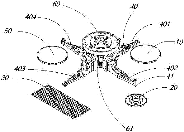
[0028] The present invention provides a glue-coated crystal-bonding equipment. In order to make the purpose, technical solution and effect of the present invention more clear and definite, the present invention will be further described in detail below with reference to the accompanying drawings and examples. It should be understood that the specific embodiments described here are only used to explain the present invention, not to limit the present invention.

[0029] See figure 1 , figure 1 It is a structural schematic diagram of the glue-covered crystal-bonding equipment of the present invention.

[0030] Such as figure 1 As shown, the glue-covered crystal-bonding equipment includes:

[0031] Wafer disc 10, used for placing crystal grains.

[0032] The glue disc 20 is used for glueing the bottom coating glue of the die.

[0033] The carrier 30 is used to provide the crystal grain to be solidified.

[0034] The die-bonding arm 40 is used to pick up the crystal grains on...


PUM


Abstract

The invention discloses a glue-coated crystal-bonding device, comprising: a wafer plate, used for placing crystal grains to be solidified; Provide the die-bonding position for the die; the die-bonding arm is used to pick up the die, and send the die to the glue tray station through the die-bonding arm for glue processing, and then pass through the die-bonding arm Bonding the glue-treated crystal grains to the positions to be solidified on the carrier. A single robotic arm is used to complete a process (including picking up crystals, taking glue, and bonding crystals), which solves the problems of timing and structural space in traditional processes, and greatly improves equipment production capacity by adding work units. At the same time, the most important thing is to solve traditional processes. The height-to-diameter ratio of each dispensing glue, the interaction between dispensing accuracy and die-bonding accuracy, poor consistency of glue dot shape, thickness, and size, and difficult control of thickness, causing problems such as blind spots or poor firmness on the bonding surface.

Description

technical field [0001] The invention relates to the field of semiconductor precision manufacturing and equipment, in particular to a glue-covered die-bonding equipment for IC and LED semiconductor packaging. Background technique [0002] Die bonder (or chip bonder) is a high-precision automatic packaging equipment that bonds chips and carriers to form thermal or electrical paths. In view of the limitations of the traditional die-bonding process, the current international leading semiconductor packaging manufacturers still use the traditional glue dispensing and die-bonding mechanism to execute the process successively to bond the chip to the target area, so that a thermal path or an electrical path is formed between the chip and the carrier. Therefore, equipment packaging manufacturers also continuously improve the structure, control, and drive of the die-bonding equipment based on this process. However, after years of hard work, the speed of the die-bonding equipment based ...

Claims


Application Information

Patent Timeline
Patent Type & Authority Patents(China)
IPC IPC(8): H01L21/56H01L21/67
Inventor 孙亚雷米广辉罗尚峰
Owner 深圳翠涛自动化设备股份有限公司
Why Eureka
Try Eureka