A display substrate, its preparation method, and a display device

A technology for displaying substrates and substrates, which is applied in the fields of final product manufacturing, sustainable manufacturing/processing, semiconductor/solid-state device manufacturing, etc. bad effect

Active Publication Date: 2021-11-30
BOE TECH GRP CO LTD
View PDF0 Cites 0 Cited by
  • Summary
  • Abstract
  • Description
  • Claims
  • Application Information

AI Technical Summary

Problems solved by technology

[0006] The purpose of the embodiments of the present invention is to provide a display substrate and its preparation method, and a display device, so as to solve the problem caused by the excessive step difference between the empty area and other areas.

Method used


Image

  • A display substrate, its preparation method, and a display device
  • A display substrate, its preparation method, and a display device
  • A display substrate, its preparation method, and a display device

Examples


preparation example Construction

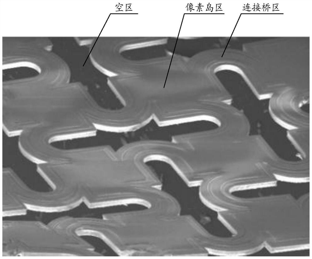
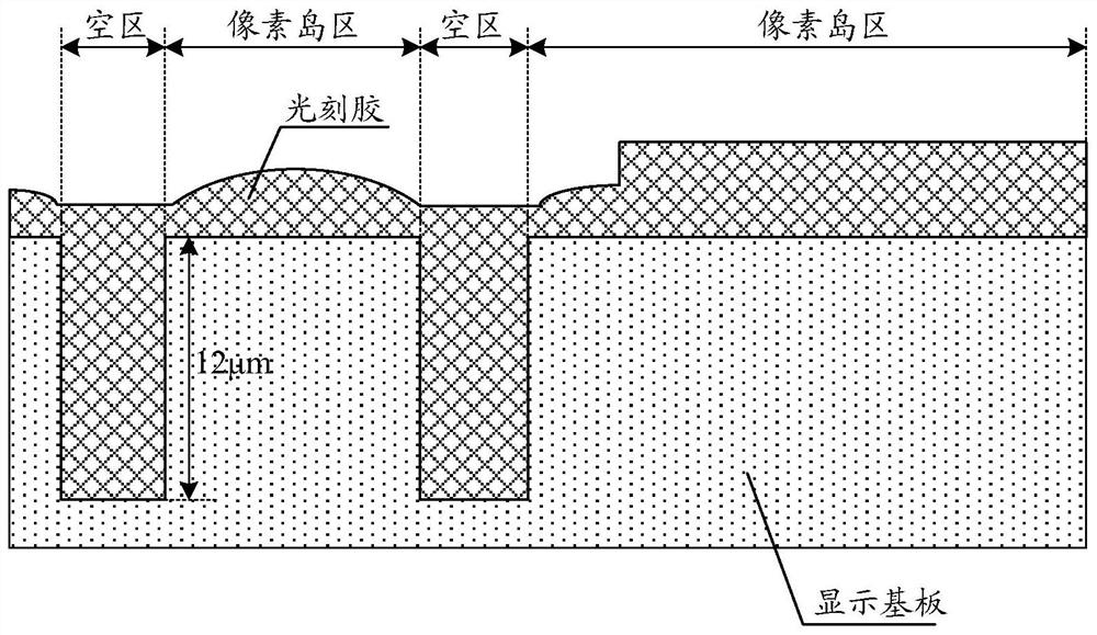
[0062] In order to solve the above technical problems, an embodiment of the present invention proposes a method for preparing a display substrate. The display substrate includes a plurality of pixel island regions, empty regions arranged between adjacent pixel island regions, and connecting bridge regions connecting adjacent pixel island regions. The preparation method of the display substrate includes:

[0063] Provide a hard substrate;

[0064] A first groove and a second groove are formed on one side of the substrate, the first groove corresponds to the pixel island region, and the second groove corresponds to the connection bridge region;

[0065] The display substrate is prepared on the side of the substrate where the first groove and the second groove are formed, the pixel island area is located in the first groove area, and the connection bridge area is located in In the second groove area, the empty area is located in an area outside the first groove and the second gr...

no. 1 example

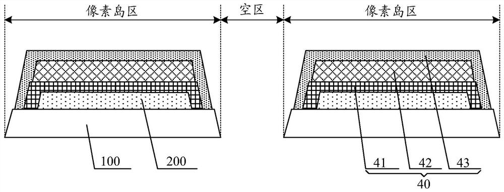
[0070] The first embodiment of the present invention provides a method for preparing a display substrate. The display substrate includes a plurality of pixel island regions, empty regions arranged between adjacent pixel island regions, and connecting bridge regions connecting adjacent pixel island regions. The island area is provided with a light-emitting unit, and the connecting lines between adjacent pixel islands are arranged in the connecting bridge area.

[0071] Figure 4 It is a schematic diagram showing the preparation method of the substrate according to the first embodiment of the present invention, such as Figure 4 As shown, the preparation method of the display substrate includes:

[0072] Provide a hard substrate;

[0073] A first groove 11 and a second groove 12 are formed on one side of the substrate, the first groove 11 corresponds to the pixel island region, the second groove 12 corresponds to the connection bridge region, and the first groove 11 and the se...

no. 2 example

[0109] The second embodiment of the present invention proposes a method for preparing a display substrate. Figure 8 It is a schematic diagram of the structure after the first groove and the second groove are formed on one side of the substrate according to the second embodiment of the present invention. Different from the first embodiment, in this embodiment, the depth of the first groove 11 is w1, and the depth of the second groove 12 is w2. In this embodiment, w1

[0110] Figure 9 It is a schematic diagram of the structure after the base is formed on the substrate in the second embodiment of the present invention. In this embodiment, the substrate 20 is a flexible substrate, and the substrate 20 has a first thickness m1 corresponding to the first groove 11, a second thickness m2 corresponding to the second groove 12, and a thickness m2 corresponding to the first groove 11 and the second groove. The area outside the groove 12 corresponds to the third thickness m3. S...


PUM

PropertyMeasurementUnit
thicknessaaaaaaaaaa
thicknessaaaaaaaaaa
thicknessaaaaaaaaaa

Abstract

The invention discloses a display substrate, a preparation method thereof, and a display device. The display substrate includes a plurality of pixel island regions, empty regions and connection bridge regions. The preparation method includes: providing a hard substrate; forming a first groove and a second groove on one side of the substrate, the first groove Corresponding to the pixel island region, the second groove corresponds to the connecting bridge region; the display substrate is prepared on the side of the substrate where the first groove and the second groove are formed, and the pixel island region is located in the first In the groove area, the connecting bridge area is located in the second groove area, and the empty area is located in the area outside the first groove and the second groove; separating the substrate from the display substrate to obtain The display substrate. In the process of preparing the display substrate by using the method, the step difference between the empty area and other areas is greatly reduced, avoiding film residue in the hollow area in the subsequent process, avoiding defects caused by poor local disconnection, and improving the yield of the display substrate.

Description

technical field [0001] The invention relates to the field of display technology, in particular to a display substrate, a preparation method thereof, and a display device. Background technique [0002] Organic Electroluminescent Display (OLED / LED) has gradually become the mainstream in the field of display due to its low power consumption, high color saturation, wide viewing angle, thin thickness, and flexibility. Applied to terminal products such as smartphones, tablets, and TVs. Among them, flexible OLED / LED products are the most prominent, and gradually become the mainstream of OLED / LED displays because they can meet various special structures. [0003] With the development of flexible technology, the flexible display panel gradually transitions from bendable (bendable), bendable (foldable), to elastic flexible (stretchable). With the gradual increase in the requirements for device flexibility, elastic flexible panels have entered everyone's field of vision. In the exis...

Claims


Application Information

Patent Timeline
Patent Type & Authority Patents(China)
IPC IPC(8): H01L27/32H01L51/52H01L51/56H01L27/15H01L33/52
CPCH01L33/52H01L27/156H01L2933/005H10K59/10H10K50/844H10K71/00Y02E10/549Y02P70/50H10K71/231H10K71/80H10K59/131H10K77/111H10K59/1201
Inventor 田宏伟牛亚男赵梦王品凡刘政
Owner BOE TECH GRP CO LTD
Why Eureka
Try Eureka