A kind of manufacturing method of TFT backplane

A manufacturing method and backplane technology, applied in semiconductor/solid-state device manufacturing, instruments, semiconductor devices, etc., can solve problems such as color distortion, achieve the effect of improving color distortion and improving competitiveness

Active Publication Date: 2021-10-08
合肥领盛电子有限公司
View PDF0 Cites 0 Cited by
  • Summary
  • Abstract
  • Description
  • Claims
  • Application Information

AI Technical Summary

Problems solved by technology

[0004] The purpose of the present invention is to provide a method for manufacturing a TFT backplane. The TFT backplane manufactured by this method can effectively improve the problem in the prior art that the liquid crystal display screen will have different degrees of color distortion when viewed from different angles of view.

Method used


Image

  • A kind of manufacturing method of TFT backplane

Examples


Embodiment Construction

[0026] In order to facilitate those skilled in the art to understand the technical solution of the present invention, the technical solution of the present invention will be further described in conjunction with the accompanying drawings.

[0027] A method for manufacturing a TFT backplane, comprising the following steps:

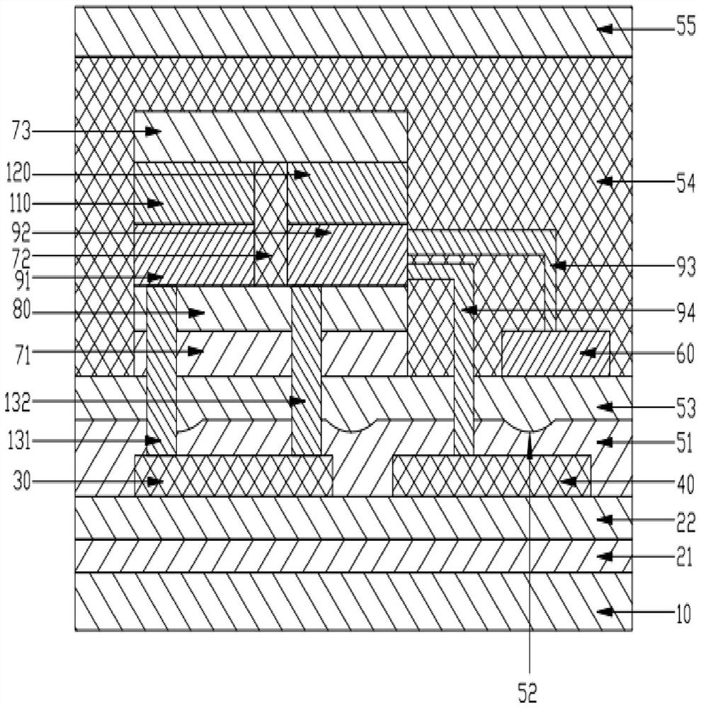
[0028] In the first step, a base substrate 10 is prepared. Then a first buffer layer 21 is formed on the base substrate 10 , and a second buffer layer 22 is formed on the first buffer layer 21 .

[0029] In the second step, several gates 30 and pixel electrodes 40 are formed on the second buffer layer 22 , and the gates 30 and pixel electrodes 40 are arranged at intervals.

[0030] In the third step, a first insulating layer 51 is formed on the surface of the non-covered area of ​​the second buffer layer 22 and the surface of the gate 30 and the pixel electrode 40, and several arc-shaped recesses 52 are uniformly arranged on the first insulating layer 51. ...


PUM


Abstract

The invention discloses a method for manufacturing a TFT backplane, which includes preparing a base substrate 10, forming a first buffer layer 21 on the base substrate 10, and forming a second buffer layer on the first buffer layer 21. 22. Form a plurality of gates 30 and pixel electrodes 40 on the second buffer layer 22, and the gates 30 and pixel electrodes 40 are arranged at intervals; the manufacturing method of the TFT backplane of the present invention uses pixel electrodes on the substrate Electric fields with unequal strengths are formed in the same pixel area of ​​the substrate, which effectively improves the color distortion of large-size liquid crystal displays at large viewing angles and improves the competitiveness of the product.

Description

technical field [0001] The invention relates to the field of display technology, in particular to a method for manufacturing a TFT backplane. Background technique [0002] In the field of display technology, flat panel displays such as Liquid Crystal Display (LCD) and Active Matrix Organic Light-Emitting Diode (AMOLED) have gradually replaced cathode ray tubes (Cathode Ray Tubes). ) displays are widely used in LCD TVs, mobile phones, personal digital assistants, digital cameras, computer screens or laptop screens, etc. The display panel is an important part of LCD and OLED displays. Whether it is an LCD display panel or an OLED display panel, it usually has a thin film transistor (Thin Film Transistor, TFT) substrate. Taking the LCD display panel as an example, it is mainly composed of a TFT substrate, a color filter (Color Filter, CF) substrate, and a liquid crystal layer (Liquid Crystal Layer) arranged between the two substrates. A driving voltage is applied to the subs...

Claims


Application Information

Patent Timeline
Patent Type & Authority Patents(China)
IPC IPC(8): H01L21/77H01L27/12G02F1/1362G02F1/1368
CPCG02F1/136227G02F1/1368H01L27/1214H01L27/1259
Inventor 魏雪王忠雷
Owner 合肥领盛电子有限公司
Why Eureka
Try Eureka