Process for producing contacts on electrical components suitable for flip-chip assemble
A technology of electrical components and flip-chip method, which is applied in the manufacture of electrical components, electrical solid devices, semiconductor/solid devices, etc., and can solve problems such as enlargement and finger structure short circuit
- Summary
- Abstract
- Description
- Claims
- Application Information
AI Technical Summary
Problems solved by technology
Method used
Image
Examples
Embodiment Construction
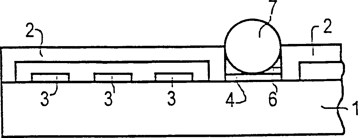
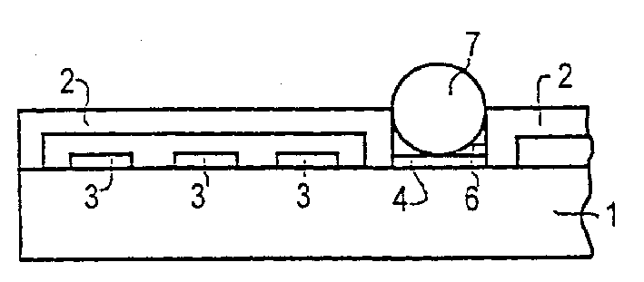
[0014] according to figure 1 An OFW element generally consists of a piezoelectric substrate 1 and conductive structures 3 arranged thereon, wherein finger electrodes such as interdigital transducers, resonators or reflectors are involved. As described in the earlier German patent entry mentioned at the outset, the conductive structure 3 is covered by a cover layer 3, which protects the structure from environmental influences, while the element with the cover layer 2 and the substrate 1 as "housing" can directly into use.
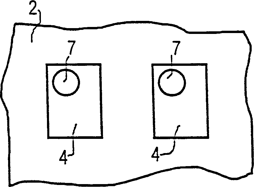
[0015] Contacts suitable for flip-chip assembly are designed according to the invention for making electrical contact with the conductive structure 3 . Such as figure 1 It can be clearly seen from the illustration that an opening 6 is provided in the cover layer 2, through which the solderable layer 4 is applied, which is in contact with the connection surface (solder pad) (not shown) of the conductive structure 3 . Such as figure 2 It is clearly shown ...
PUM
 Abstract
Description
Claims
Application Information


