Semiconductor packaging mold and packaging technology thereof

A semiconductor and mold technology, applied in semiconductor/solid-state device manufacturing, electrical components, circuits, etc., can solve the problems of incomplete protection of semiconductor chips, inability to meet the rapid positioning of semiconductor chips of different sizes, etc., to facilitate heat dissipation and improve service life Effect

Active Publication Date: 2019-12-10
东和半导体设备(南通)有限公司
View PDF6 Cites 5 Cited by
  • Summary
  • Abstract
  • Description
  • Claims
  • Application Information

AI Technical Summary

Problems solved by technology

[0002] Semiconductor packaging refers to encapsulating and protecting semiconductor chips with protective shells. The existing packaging devices do not provide comprehensive protection for semiconductor chips, and cannot meet the rapid positioning of semiconductor chips of different sizes. Therefore, we propose a semiconductor packaging mold and Its packaging process to solve the problems mentioned in the background technology above

Method used


Image

  • Semiconductor packaging mold and packaging technology thereof
  • Semiconductor packaging mold and packaging technology thereof
  • Semiconductor packaging mold and packaging technology thereof

Examples


Embodiment 1

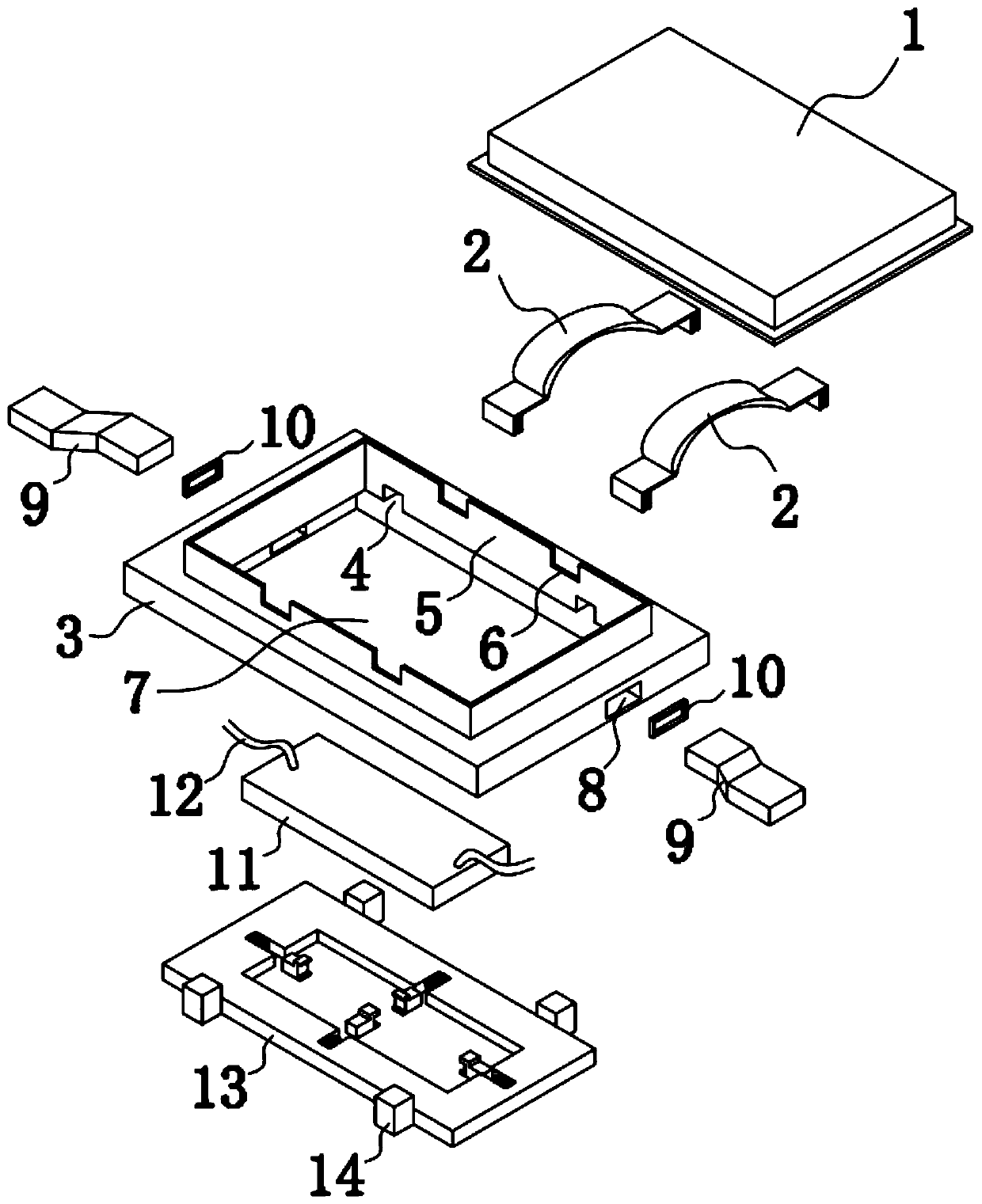
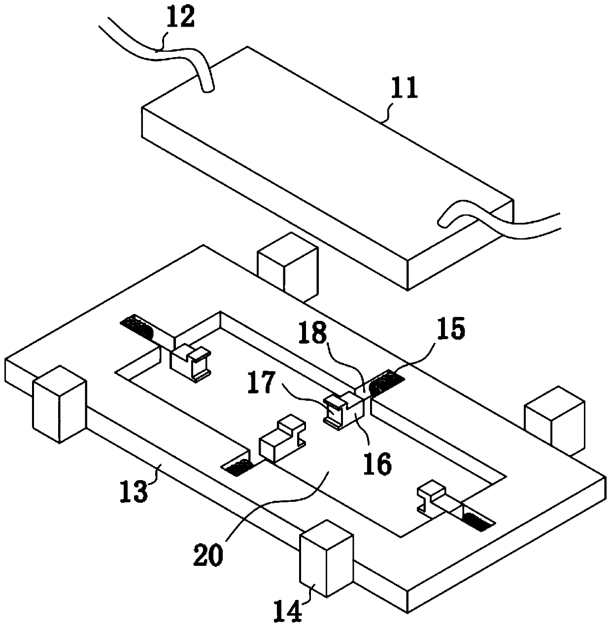
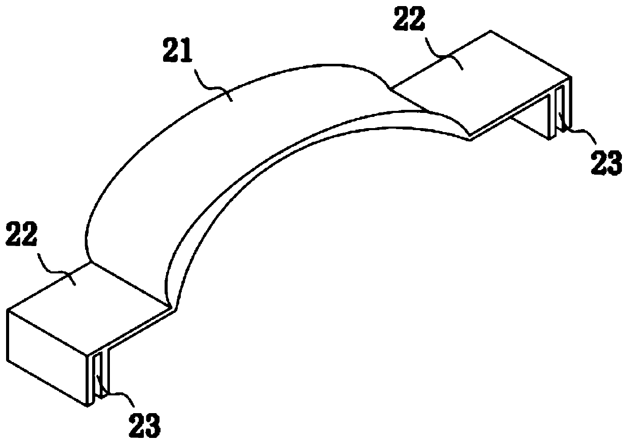
[0024] The present invention provides such Figure 1-4 A semiconductor package mold, comprising a semiconductor chip 11 and a mounting plate 3, the semiconductor chip 11 is arranged in the mounting groove 20 on the upper end of the substrate 13, and fixed by a clamping mechanism in the mounting groove 20, the mounting plate 3 The middle part of the opening groove 7 is provided with an opening groove 7, the upper end of the opening groove 7 is provided with a protective ring 5, the lower end of the mounting plate 3 is provided with a positioning groove 4, and the positioning protrusion 14 on the side of the substrate 13 is snapped into the positioning In the groove 4, pins 9 are connected to the sockets 8 at both ends of the mounting plate 3, and one end of the pins 9 extending into the opening groove 7 is connected to the semiconductor chip 11 through a lead wire 12, and the protective ring 5 There are two sets of transverse support mechanisms 2 connected between the front and...


PUM


Abstract

The invention discloses a semiconductor packaging mold. The mold comprises a semiconductor chip and an installation plate. The semiconductor chip is arranged in an installation groove of an upper endof a substrate and is fixed through a clamping mechanism in the installation groove. An open groove is arranged in the middle of the installation plate. A positioning groove is arranged in a lower endof the installation plate. A positioning embossment of a side edge of the substrate is clamped in the positioning groove. Pins are connected to insertion ports of two ends of the installation plate.One end, extending into the open groove, of each pin is connected to the semiconductor chip through a lead, two sets of transverse supporting mechanisms are connected between a front side wall and a rear side wall of a protection ring, an outer side of the protection ring is covered by a packaging cover, and a protruding ring integrally formed with the packaging cover is arranged on the lower endof the packaging cover in a circle. In the invention, rapid fixation of the semiconductor chips with different sizes is satisfied; and heat dissipation of the semiconductor chip is facilitated, a service life of the semiconductor chip is prolonged, and the semiconductor chip is protected in all directions.

Description

technical field [0001] The invention belongs to the technical field of semiconductors, and in particular relates to a semiconductor packaging mold, and also relates to a packaging process of the semiconductor packaging mold. Background technique [0002] Semiconductor packaging refers to encapsulating and protecting semiconductor chips with protective shells. The existing packaging devices do not provide comprehensive protection for semiconductor chips, and cannot meet the rapid positioning of semiconductor chips of different sizes. Therefore, we propose a semiconductor packaging mold and Its packaging process is to solve the problems mentioned in the above-mentioned background technology. Contents of the invention [0003] The object of the present invention is to provide a semiconductor packaging mold and its packaging process, so as to solve the problems raised in the above-mentioned background technology. [0004] In order to achieve the above object, the present inve...

Claims


Application Information

Patent Timeline
Patent Type & Authority Applications(China)
IPC IPC(8): H01L21/56
CPCH01L21/565
Inventor 童华
Owner 东和半导体设备(南通)有限公司
Why Eureka
Try Eureka