Configurable image data caching system based on FPGA and DDR3 SDRAM
A technology of image data and cache system, which is applied in the direction of memory system, electrical digital data processing, memory architecture access/allocation, etc. It can solve problems such as complex operation, slow data transmission rate, and long development cycle, and achieve the effect of convenient configuration
- Summary
- Abstract
- Description
- Claims
- Application Information
AI Technical Summary
Problems solved by technology
Method used
Image
Examples
Embodiment Construction
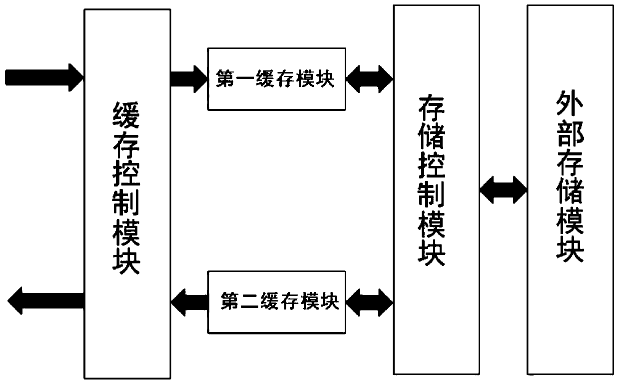
[0029] Such as figure 1 As shown, the present invention discloses a configurable image data cache system based on FPGA and DDR3 SDRAM, the system is built on the FPGA platform, including an external storage module, a storage control module, a first cache module, a second cache module and a cache control module ,in:
[0030] The external storage module is used to store image data.
[0031] In this embodiment, the external storage module adopts DDR3 SDRAM. DDR3 has the characteristics of high bandwidth, high reliability, low power consumption and low cost. It is composed of 8 128MB particles and the memory is 1GB. The data bit width of each storage particle is 8bit, and 8 pieces are put together to form a memory strip with a data bit width of 64bit. In addition, the burst length is set to 8, so the data bit width of each read and write can reach 512bit , greatly improving the read and write efficiency of DDR3. DDR3 can work at an interface frequency of 800MHz, and the transmi...
PUM
 Abstract
Description
Claims
Application Information


