


Quick Research
Generate reliable direction feasibility study reports for your R&D in just a few steps.

Technical Q&A
Discover and master advanced knowledge NOW. Basics, ideas, possibilities, all at once.

Find Solutions
As an expert in R&D theories, this can generate solutions to your technical problems instantly.

Evaluate Feasibility
Analyze your overall solution with one click, know your potential R&D risks in advance.

Monitor Landscape
Get weekly tech updates, stay abreast of the latest tech innovations and key insights.
Power supply apparatus and image forming apparatus
一种电源装置、图像的技术,应用在应用电荷图形的电记录工艺、应用电荷图形的电记录工艺的设备、输出功率的转换装置等方向,能够解决FETQ101振荡频率变低等问题
- Summary
- Abstract
- Description
- Claims
- Application Information
AI Technical Summary
Problems solved by technology
Method used
Image

Examples
example 1
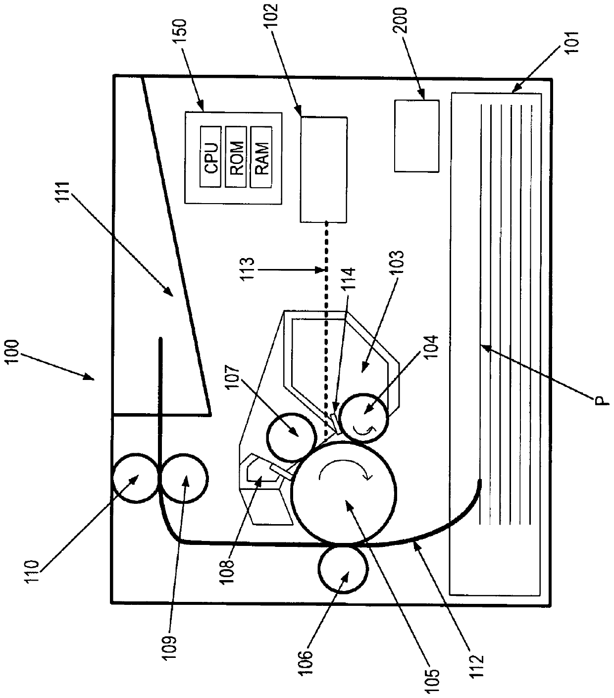
[0026] The power supply device of the present invention is applied to, for example, an image forming apparatus. Therefore, first, a laser printer as a type of image forming apparatus will be described.
[0027] [Configuration of Image Forming Apparatus]
[0028] figure 1 A cross-sectional view of a monochrome laser printer (hereinafter referred to as a printer) 100 in Example 1 is illustrated. The printer 100 includes a sheet feeding unit 101, a laser scanner 102 as an exposure device, a toner tank 103, a developing roller 104 as a developing device, a photosensitive drum 105 as a photosensitive member, a transfer roller 106 as a transfer device, A charging roller 107 and a waste toner tank 108 . Further, the printer 100 includes a fixing roller 109 , a pressure roller 110 , a discharge unit 111 , a conveying path 112 , and a developing blade 114 . The sheet feeding unit 101 is a sheet feeding unit that stores recording media (for example, paper P) on which printing is to...
example 3
[0052] [Setting of pulse signal and PWM signal]
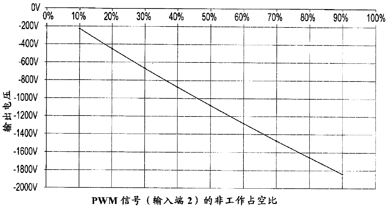
[0053] In Examples 1 and 2, it has been described that the frequency or duty cycle of the pulse signal input to the input terminal 1 is changed according to the voltage value to be output or the assumed load. However, the frequency or duty cycle of the pulse signal input to the input terminal 1 can be changed according to the time-varying load.
[0054] E.g, figure 1 The printer 100 in forms an image in a series of operations, as shown in Example 1. Therefore, for example, the timing at which the fed paper P contacts the photosensitive drum 105 can be predicted. Since the paper P, which is a resistor, enters the position where the transfer roller 106 and the photosensitive drum 105 were in contact with each other before then, it looks like the load resistance becomes high at this time from the viewpoint of the high-voltage power supply. Note that the load at this time refers to the transfer load. As described above, the ri...
example 4
[0058] [Setting of pulse signal and PWM signal]
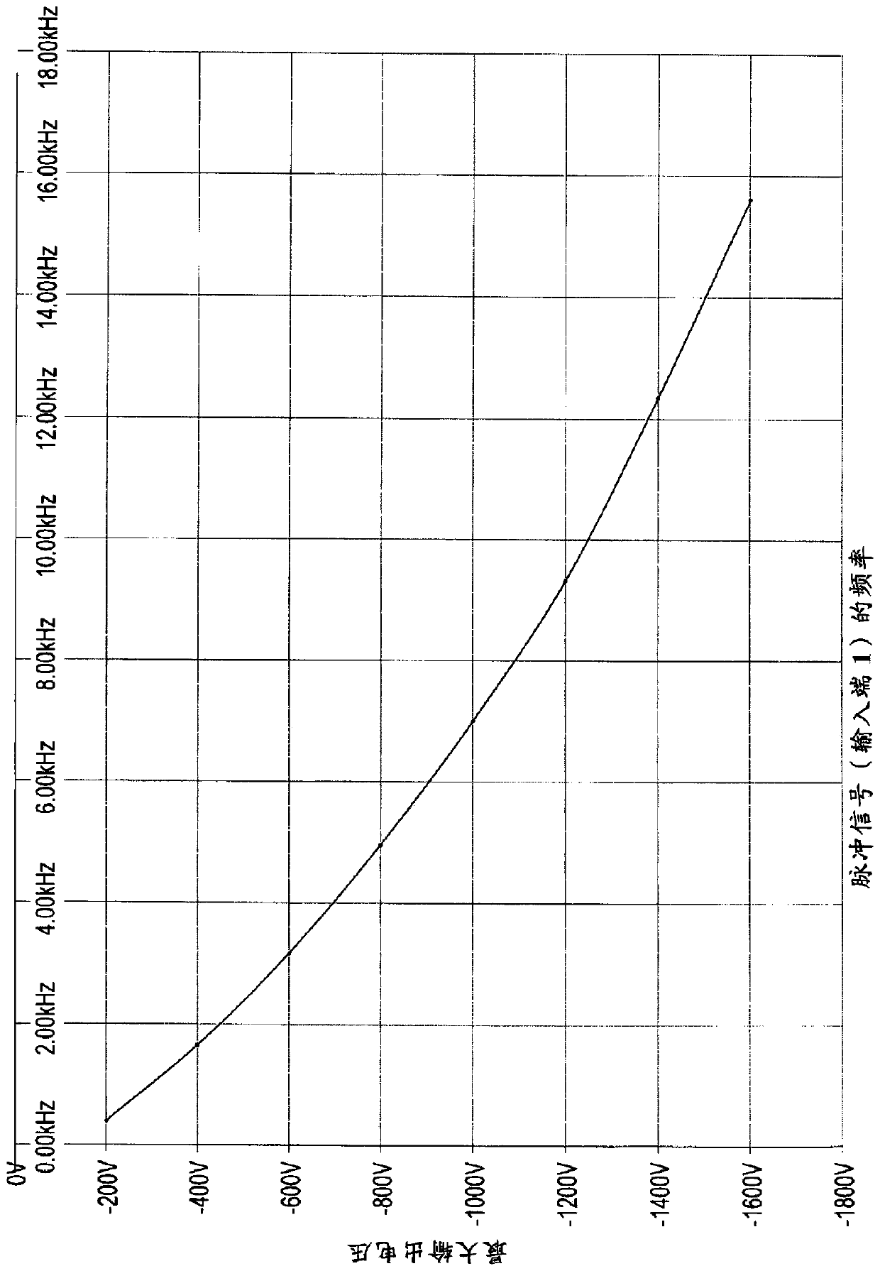
[0059] There are other situations where it is advantageous to vary the frequency of the pulse signal input to input 1 . For example, by temporarily increasing the frequency of the pulse signal when the output voltage rises, the time to reach the target voltage can be shortened. The situation is Figure 5A with Figure 5B shown in . Figure 5A shows the time variation of the output voltage, Figure 5B The time variation of the frequency of the pulse signal input to the input terminal 1 is illustrated. Figure 5A Also illustrated are times T1 and T2 when both output voltages rise to the target voltage. The two time axes are the same, and the one-dot chain line indicates the same timing t1. Also, a solid line indicates a case where the frequency of the pulse signal input to the input terminal 1 is fixed at 5 kHz, and a thick dashed line indicates a case where the pulse signal moves at double frequency (ie, 10 kHz) for a peri...
PUM
 Abstract
Description
Claims
Application Information
 - R&D Engineer
- R&D Manager
- IP Professional
- Industry Leading Data Capabilities
- Powerful AI technology
- Patent DNA Extraction
Browse by: Latest US Patents, China's latest patents, Technical Efficacy Thesaurus, Application Domain, Technology Topic, Popular Technical Reports.
© 2024 PatSnap. All rights reserved.Legal|Privacy policy|Modern Slavery Act Transparency Statement|Sitemap|About US| Contact US: help@patsnap.com