Chip package clamping device
A clamping device and chip packaging technology, which is applied in the direction of electrical components, semiconductor/solid-state device manufacturing, circuits, etc., can solve problems such as low production efficiency, unsuitable semiconductor packaging automation process, misalignment, etc., to improve processing efficiency and save clamping Fixed time, simple structure effects
- Summary
- Abstract
- Description
- Claims
- Application Information
AI Technical Summary
Problems solved by technology
Method used
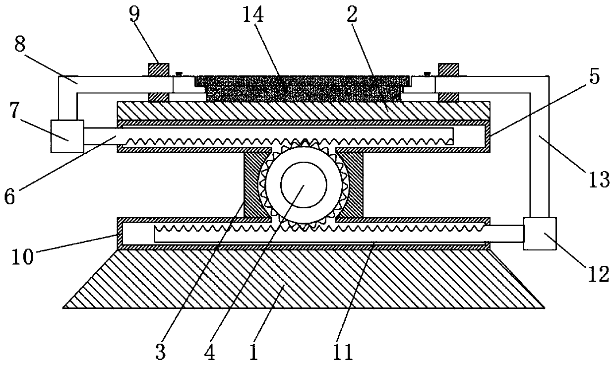
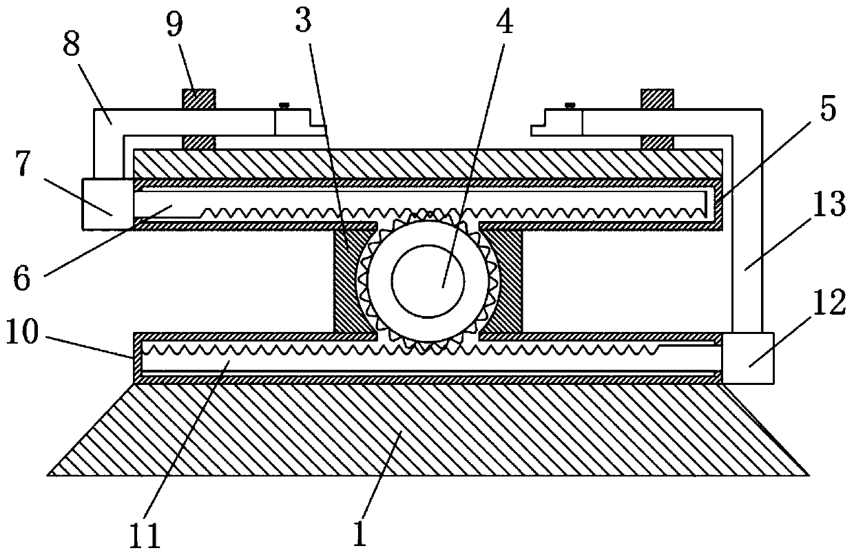
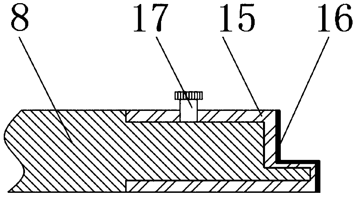
Image

Examples
Embodiment Construction
[0018] The technical solutions in the embodiments of the present invention will be clearly and completely described below in conjunction with the accompanying drawings in the embodiments of the present invention. Obviously, the described embodiments are only a part of the embodiments of the present invention, rather than all the embodiments.
[0019] Examples of embodiments are shown in the drawings, in which the same or similar reference numerals indicate the same or similar elements or elements with the same or similar functions throughout. The embodiments described below with reference to the accompanying drawings are exemplary, and are intended to explain the present invention, but should not be construed as limiting the present invention.
[0020] In the description of the present invention, it should be understood that the terms "center", "longitudinal", "transverse", "length", "width", "thickness", "upper", "lower", "front", " Back", "Left", "Right", "Vertical", "Horizontal"...
PUM
 Abstract
Description
Claims
Application Information
PatSnap Eureka turns technology decisions into work you can execute. Powered by our Innovation Knowledge Graph, it runs expert workflows across engineering, life sciences, materials and intellectual property. Get your review-ready output in minutes.


