Preparation method of salient points with different specifications and sizes

A bump and size technology, used in semiconductor/solid-state device manufacturing, electrical components, electrical solid-state devices, etc., can solve problems such as growing bumps of different sizes, and achieve the effect of reducing production costs and cycles and improving production efficiency.

Pending Publication Date: 2019-12-20
58TH RES INST OF CETC
View PDF0 Cites 0 Cited by
  • Summary
  • Abstract
  • Description
  • Claims
  • Application Information

AI Technical Summary

Problems solved by technology

[0004] The purpose of the present invention is to provide a method for preparing bumps of different specifications and sizes, so as to solve the problem that it is difficult to grow bumps of different sizes in the same wafer or the same chip in the wafer-level bump growth process

Method used


Image

  • Preparation method of salient points with different specifications and sizes
  • Preparation method of salient points with different specifications and sizes
  • Preparation method of salient points with different specifications and sizes

Examples


Embodiment 1

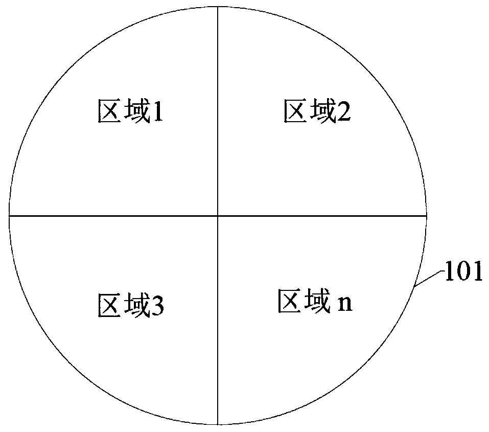
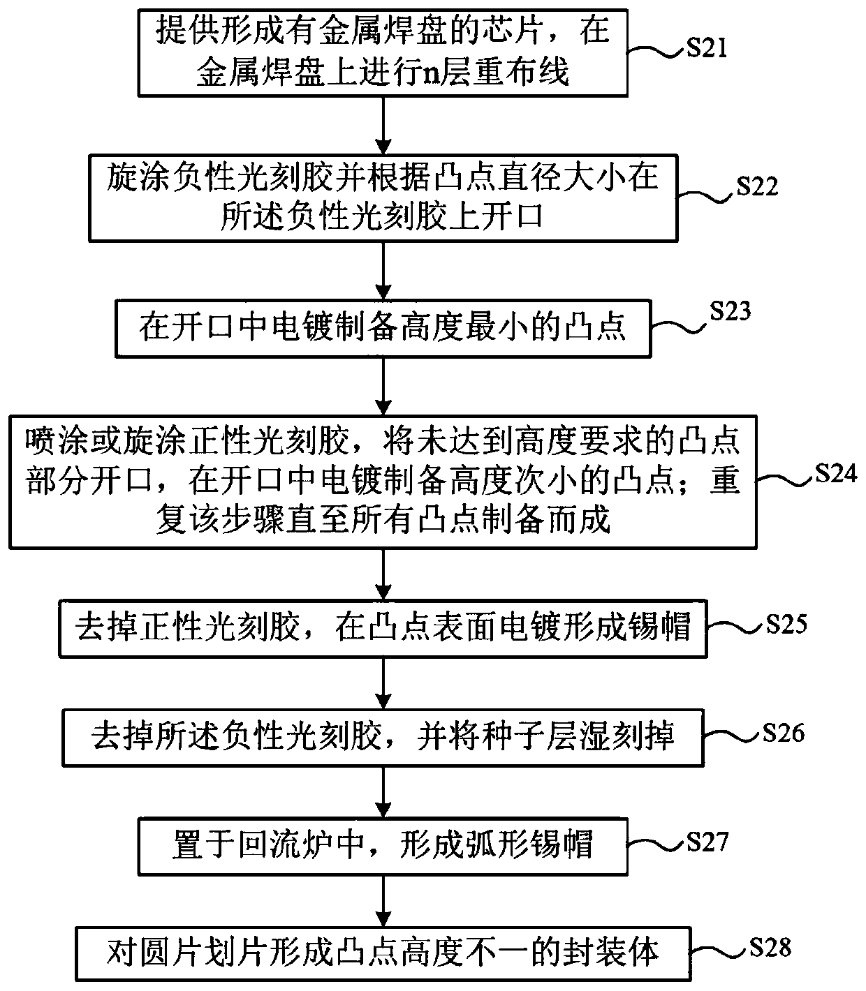
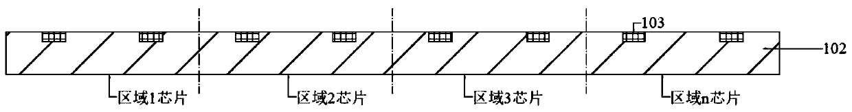
[0043] figure 1 It is an MPW wafer, including wafer 101, in which different chips are distributed in different regions, the size of the chip bumps in each region is the same, and the height of the chip bumps in different regions is different. The invention provides a method for preparing bumps with different specifications and sizes, and the process is as follows figure 2 As shown, including the following steps:

[0044] Step S21, providing a chip formed with metal pads, and performing n-layer rewiring on the metal pads;

[0045] Step S22, spin-coating a negative photoresist and make openings on the negative photoresist according to the diameter of the bumps;

[0046] Step S23, electroplating in the opening to prepare bumps with the smallest height;

[0047] Step S24, spraying or spin-coating positive photoresist, opening the bumps that do not meet the height requirement, and electroplating in the openings to prepare bumps with the next smallest height; repeat this step until all bum...


PUM

PropertyMeasurementUnit
thicknessaaaaaaaaaa
thicknessaaaaaaaaaa
heightaaaaaaaaaa

Abstract

The invention discloses a preparation method of salient points with different specifications and sizes, and belongs to the technical field of integrated circuit packaging. The method comprises the following steps of: firstly, providing a chip on which a metal bonding pad is formed, and carrying out n-layer rewiring on the metal bonding pad; spin-coating negative photoresist and forming an openingin the negative photoresist according to the diameter of the salient point; performing electroplating to prepare the salient point with the minimum height in the opening; spraying or spin-coating a positive photoresist so that the convex points which do not meet the height requirement are partially opened, and preparing the convex points with the secondary small height in the openings through electroplating; repeating the step until all the salient points are prepared; removing the positive photoresist, and electroplating the surfaces of the salient points to form tin caps; removing the negative photoresist, and carrying out wet etching on the seed layer; placing the product in a reflow oven to form an arc-shaped tin cap; and scribing the wafer to form packaging bodies with different salient point heights. The special requirement for growth of the salient points of different sizes on the MPW wafer level is met, and the problem that the salient points of different sizes grow in the samechip in the wafer level salient point growth process is solved.

Description

Technical field [0001] The invention relates to the technical field of integrated circuit packaging, in particular to a method for preparing bumps with different specifications and sizes. Background technique [0002] In recent years, with the continuous progress of living standards and technology, digital electronic products have increasingly higher requirements for miniaturization, high bandwidth and intelligence. In order to meet these needs, industry manufacturers are constantly seeking and creating various new technologies. At present, the more commonly used packaging methods to improve product performance are mainly three-dimensional stacking technologies, such as TSMC's CoWos, InFO, and Intel's EMIB. For three-dimensional packaging, high-density bumps are indispensable for high-speed and high-bandwidth transmission of heterogeneous chips. At present, bumps are mainly divided into two categories: solder ball bumps and copper pillar bumps. Compared with solder ball bumps,...

Claims


Application Information

Patent Timeline
Patent Type & Authority Applications(China)
IPC IPC(8): H01L21/60H01L23/488
CPCH01L24/11H01L24/14H01L2224/1111H01L2224/11462H01L2224/11831H01L2224/1403H01L2224/1411H01L2224/11
Inventor 王成迁明雪飞吉勇
Owner 58TH RES INST OF CETC
Why Eureka
Try Eureka