Display substrate, preparation method thereof, display panel and display device

A technology for display substrates and display areas, which is used in semiconductor/solid-state device manufacturing, electrical components, and electrical solid-state devices, etc., and can solve problems such as low film uniformity

Active Publication Date: 2019-12-20
BOE TECH GRP CO LTD
View PDF10 Cites 1 Cited by
  • Summary
  • Abstract
  • Description
  • Claims
  • Application Information

AI Technical Summary

Problems solved by technology

[0004] Embodiments of the present invention provide a display substrate and its preparation method, a display panel, and a display device, which are used to solve the problem of low uniformity of film formation

Method used


Image

  • Display substrate, preparation method thereof, display panel and display device
  • Display substrate, preparation method thereof, display panel and display device
  • Display substrate, preparation method thereof, display panel and display device

Examples


Embodiment Construction

[0039] The following will clearly and completely describe the technical solutions in the embodiments of the present invention with reference to the accompanying drawings in the embodiments of the present invention. Obviously, the described embodiments are only some, not all, embodiments of the present invention. Based on the embodiments of the present invention, all other embodiments obtained by persons of ordinary skill in the art without making creative efforts belong to the protection scope of the present invention.

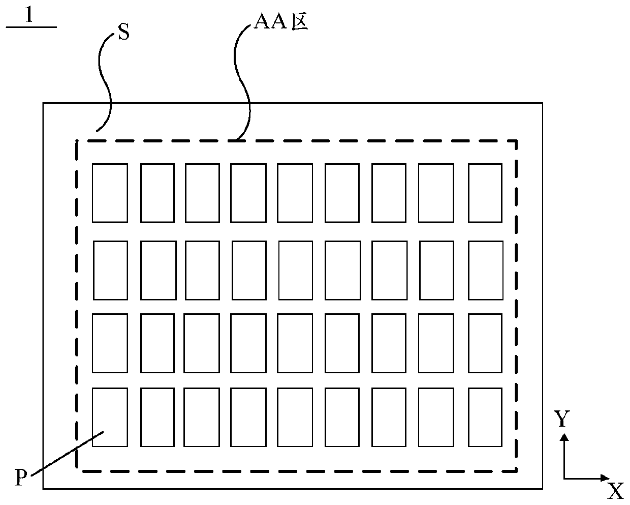
[0040] An embodiment of the present invention provides a display device, which includes a display panel 1 .

[0041] like figure 1 As shown, the display panel 1 has a display area (active area, AA area for short) and a peripheral area S, and the peripheral area S is set around the AA area, for example.

[0042] A plurality of sub-pixels P are arranged in the above-mentioned area AA. The plurality of sub-pixels P includes at least a first color sub-pixel, a s...


PUM


Abstract

The embodiment of the invention provides a display substrate, a preparation method thereof, a display panel and a display device, which relate to the technical field of display and aim to solve the problem of relatively low film forming uniformity. The display substrate comprises a substrate and a plurality of light-emitting units arranged in a display area on the substrate. The light-emitting layer in at least one light-emitting unit is manufactured by adopting an ink-jet printing process, and the distances from all points on the edge of the cross section, perpendicular to the thickness direction of the substrate, of the light-emitting layer to the center of the cross section are approximately equal.

Description

technical field [0001] The present invention relates to the field of display technology, in particular to a display substrate and a preparation method thereof, a display panel, and a display device. Background technique [0002] Compared with Liquid Crystal Display (LCD) devices, Organic Light-Emitting Diode (OLED) display devices have the advantages of self-illumination, fast response, wide viewing angle, high brightness, bright colors, and thinness. It is a hot spot for display products to pursue and adopt at present. [0003] The film forming process in the OLED display device mainly includes vacuum evaporation and solution process. Vacuum evaporation is suitable for organic small molecule materials. Its film formation is uniform and the technology is relatively mature, but the equipment cost is high and the material utilization rate is low. In addition, when producing a display device with a large light-emitting surface area, the mask plate is relatively Bit precision ...

Claims


Application Information

Patent Timeline
Patent Type & Authority Applications(China)
IPC IPC(8): H01L27/32H01L51/50H01L51/00H01L51/56
CPCH10K59/352H10K59/353H10K59/12H10K71/135H10K50/11H10K71/00H10K59/121H10K71/164H10K71/12H10K59/35H10K59/122H10K59/173
Inventor 侯文军
Owner BOE TECH GRP CO LTD
Why Eureka
Try Eureka