Blue-light perovskite light-emitting diode based on modified hole transport layer and production method thereof

A hole transport layer and light emitting diode technology, which is applied in semiconductor/solid-state device manufacturing, electrical components, circuits, etc., can solve the problems of perovskite emission wavelength shift, complex processing technology, and complicated actual operation, and achieve passivation. Perovskite defects, simple operation, and the effect of improving the uniformity of film formation

Pending Publication Date: 2021-11-02
SUZHOU UNIV
View PDF0 Cites 1 Cited by
  • Summary
  • Abstract
  • Description
  • Claims
  • Application Information

AI Technical Summary

Problems solved by technology

At present, the anti-solvent method is often used to improve the crystallization quality of perovskite films, but this method increases the complexity of the operation, and is difficult to apply to the large-area device preparation process of the industrial solution method, such as printing and inkjet printing; in The introduction of micro-nano structures into the device to enhance optical coupling can improve the light output of the device, but the processing technology is complicated and the manufacturing cost is increased; the composition adjustment of the perovskite layer is more advantageous than the previous two methods, but the actual operation is also relatively Complex, easy to cause a large shift in the emission wavelength of perovskite

Method used


Image

  • Blue-light perovskite light-emitting diode based on modified hole transport layer and production method thereof
  • Blue-light perovskite light-emitting diode based on modified hole transport layer and production method thereof
  • Blue-light perovskite light-emitting diode based on modified hole transport layer and production method thereof

Examples


preparation example Construction

[0031] As a specific embodiment, taking propanolamine as an example, the preparation method of the blue light perovskite light-emitting diode based on the modified hole transport layer of the present invention is the following detailed steps:

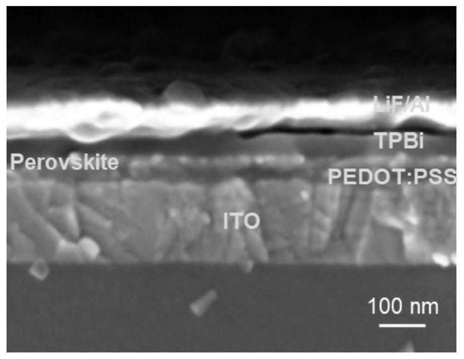
[0032] S1. Clean the anode substrate ultrasonically with diluted Decon aqueous solution, then rinse the ITO anode substrate with deionized water, then place it in ethanol and isopropanol for ultrasonic cleaning for 5-10 minutes, and finally dry it in an oven;

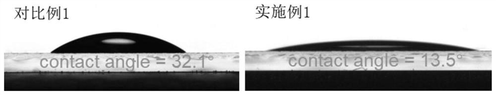
[0033] S2. mixing the propanolamine additive into the PEDOT:PSS stock solution to prepare a PEDOT:PSS solution with a doping concentration of 1-3 μl / ml;

[0034] S3. Spin-coat the PEDOT:PSS solution at 4000 rpm / min for 40 s, and then anneal at 140°C for 15 minutes at a high temperature to form a hole transport layer;

[0035] S4. In the glove box (nitrogen protection), CsBr, PbBr 2 , PbCl 2 , KBr, p-f-PEABr and formamidine hydrobromide (FABr) were dissolved in DMSO according to...

Embodiment 1

[0038] Example 1 A blue-light perovskite light-emitting diode based on a modified hole transport layer, the preparation method of which is as follows:

[0039](1) Ultrasonic clean the ITO anode substrate with a 20-fold diluted Decon aqueous solution for 5 minutes, then rinse the ITO anode substrate with deionized water, then place it in ethanol and isopropanol for 5 minutes, and finally dry it in an oven ;

[0040] (2) Add 2 μL of propanolamine to 1 mL of PEDOT:PSS stock solution to prepare a PEDOT:PSS solution with a doping concentration of 2 μl / ml;

[0041] (3) The above PEDOT:PSS solution was spin-coated on the surface of the ITO anode at 4000 rpm / min for 40 s, and then annealed at 140 °C for 15 minutes to form a hole transport layer;

[0042] (4) Mix 0.282 mmol of CsBr and 0.067 mmol of PbBr in a glove box (nitrogen protection) 2 , 0.134mmol of PbCl 2 , 0.05 mmol of KBr, 0.08 mmol of p-f-PEABr and 0.03 mmol of formamidine hydrobromide (FABr) were dissolved in 1.8 ml of ...

Embodiment 2

[0058] The difference between this embodiment and Embodiment 1 lies in that in step (1), the effective area of ​​the ITO anode substrate used is different, and the size of the light emitting area of ​​the finally manufactured device is different. In this embodiment, the light-emitting area of ​​the blue perovskite light-emitting diode based on the modified hole transport layer is 100 mm 2 . The rest of the parameters are the same. as follows:

[0059] (1) Ultrasonic clean the ITO anode substrate with a 20-fold diluted Decon aqueous solution for 5 minutes, then rinse the ITO anode substrate with deionized water, then place it in ethanol and isopropanol for 5 minutes, and finally dry it in an oven ;

[0060] (2) Add 2 μL of propanolamine to 1 mL of PEDOT:PSS stock solution to prepare a PEDOT:PSS solution with a doping concentration of 2 μl / ml;

[0061] (3) The above PEDOT:PSS solution was spin-coated on the surface of the ITO anode at 4000 rpm / min for 40 s, and then annealed...


PUM

PropertyMeasurementUnit
thicknessaaaaaaaaaa
thicknessaaaaaaaaaa
thicknessaaaaaaaaaa

Abstract

The invention relates to a blue-light perovskite light-emitting diode based on a modified hole transport layer and a production method thereof. The device comprises an anode substrate, the modified hole transport layer, a perovskite light-emitting layer, an electron transport layer and a cathode. According to the invention, the propanolamine molecular additive is creatively introduced so that the crystal growth of the blue light perovskite luminescent layer can be effectively regulated and controlled, a high-quality luminescent film with high uniformity, high crystallinity and low defect density is formed, and the photoluminescence characteristic and the spectral stability of the film are enhanced; and the brightness and the external quantum efficiency of the produced blue light perovskite light-emitting diode are obviously improved, and the service life of the produced blue light perovskite light-emitting diode is obviously prolonged. The modification method disclosed by the invention is low in cost, simple to operate, remarkable in effect and suitable for various existing preparation processes such as spin coating, blade coating, printing, ink-jet printing and the like.

Description

technical field [0001] The invention relates to the field of preparation of perovskite photoelectric devices, in particular to a method for preparing a blue perovskite light-emitting diode based on interface modification of a hole transport layer. Background technique [0002] Metal halide perovskite (Perovskite) is a popular material in international research after graphene. It has excellent photoelectric properties, low cost and solution processing, and has been widely studied in the field of optoelectronic device technology; among them, perovskite solar cells Commercial large-scale preparation has been realized, and perovskite light-emitting diodes have also achieved rapid development in the past 10 years, and have good application prospects in the fields of display and lighting. [0003] The outstanding advantages of perovskite light-emitting diodes are high color purity and solution processing. At present, the external quantum efficiency of green and red perovskite lig...

Claims


Application Information

Patent Timeline
Patent Type & Authority Applications(China)
IPC IPC(8): H01L51/50H01L51/54H01L51/56
CPCH10K85/1135H10K50/155H10K71/00
Inventor 唐建新王经坤李艳青
Owner SUZHOU UNIV
Why Eureka
Try Eureka