Display panel, display device and display panel manufacturing method
A display panel and display device technology, which is applied in semiconductor/solid-state device manufacturing, electrical components, diodes, etc., can solve problems such as light leakage, affecting imaging quality, and reducing light transmission in opening areas, so as to improve imaging quality and transmittance. Over-efficiency, the effect that contributes to mass production
- Summary
- Abstract
- Description
- Claims
- Application Information
AI Technical Summary
Problems solved by technology
Method used
Image

Examples
Embodiment Construction
[0018] Embodiments of the present invention are described in detail below, examples of which are shown in the drawings, wherein the same or similar reference numerals denote the same or similar components or components having the same or similar functions throughout. The directional terms mentioned in the present invention, such as: up, down, left, right, front, back, inside, outside, side, etc., are only directions referring to the drawings. The embodiments described below with reference to the drawings and the directional terms used are exemplary, and are only used to explain the present invention, and should not be construed as limiting the present invention.
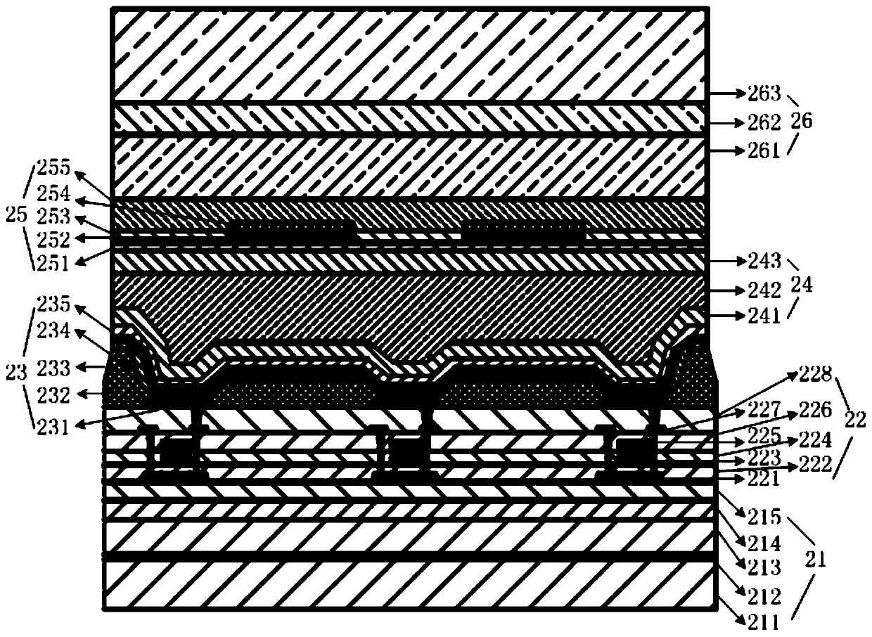
[0019] see figure 2 , a schematic diagram of the layered structure of the display area of the display panel in the prior art. The display panel is an OLED touch display panel, and its film layer structure includes a flexible substrate 21, and a thin film transistor layer 22, an organic light-emitting layer (EL) 2...
PUM
 Abstract
Description
Claims
Application Information