Array substrate, display panel and manufacturing method of array substrate

A technology of an array substrate and a manufacturing method, which is applied in the display field, can solve problems such as poor contrast, poor haze, and poor picture display effect, and achieve the effects of improving contrast, solving low haze, and increasing haze

Active Publication Date: 2019-12-31
WUHAN CHINA STAR OPTOELECTRONICS TECH CO LTD
View PDF7 Cites 5 Cited by
  • Summary
  • Abstract
  • Description
  • Claims
  • Application Information

AI Technical Summary

Problems solved by technology

[0004] However, the thickness of the liquid crystal layer in the under-screen camera area of ​​the existing display panel is about three microns, and its haze is poor, which affects its poor contrast and poor picture display effect.

Method used


Image

  • Array substrate, display panel and manufacturing method of array substrate
  • Array substrate, display panel and manufacturing method of array substrate
  • Array substrate, display panel and manufacturing method of array substrate

Examples


Embodiment Construction

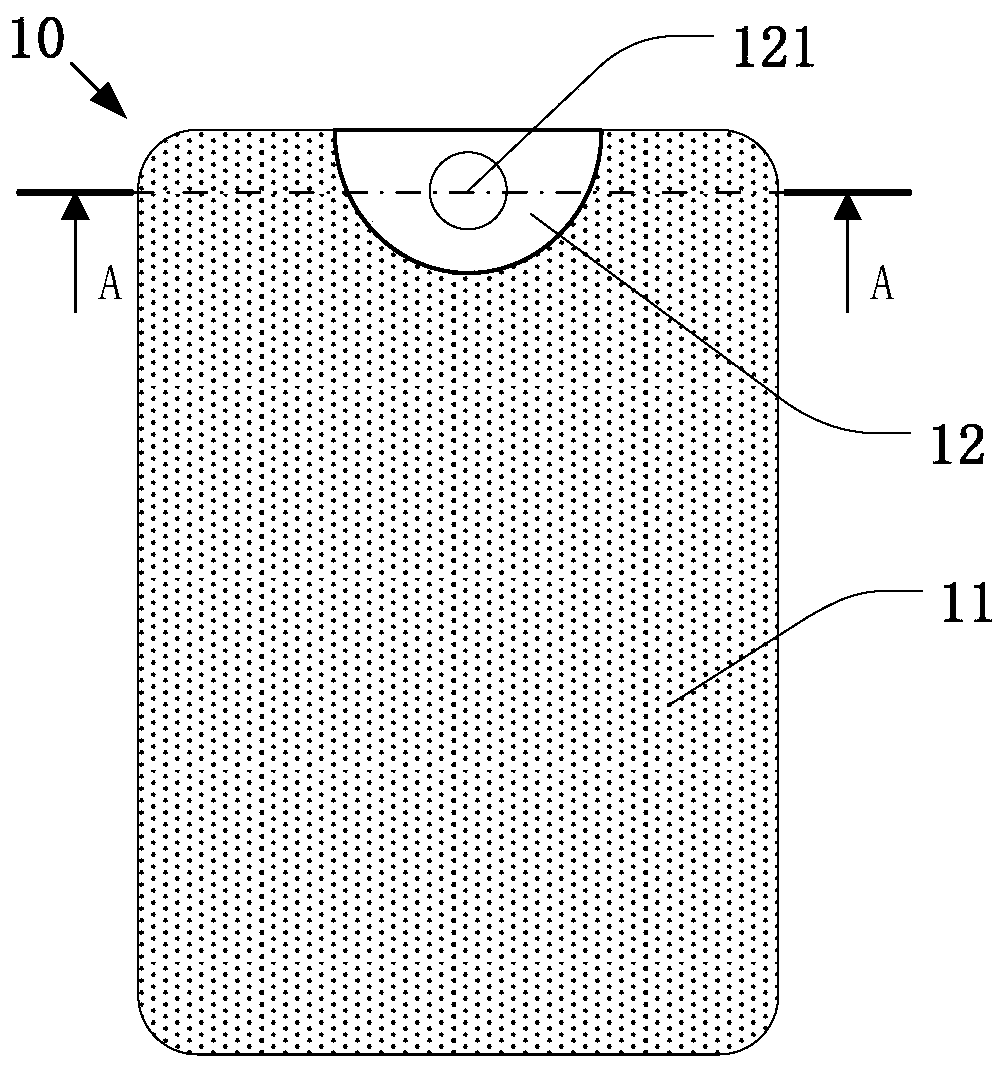
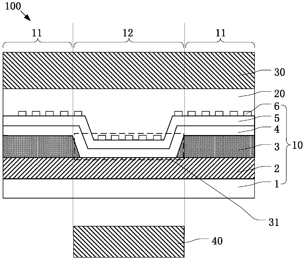
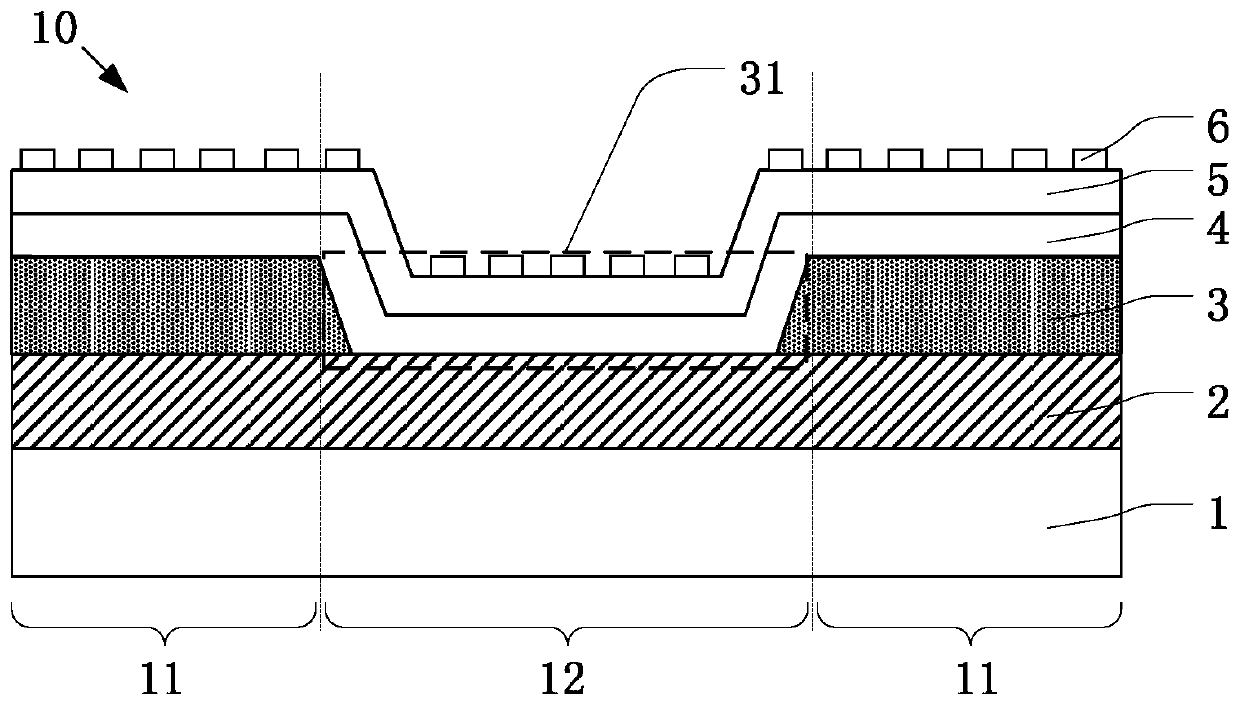
[0033] The following descriptions of the various embodiments refer to the accompanying drawings to illustrate specific embodiments in which the invention may be practiced. The directional terms mentioned in the present invention, such as [top], [bottom], [front], [back], [left], [right], [inside], [outside], [side], etc., are only for reference The orientation of the attached schema. Therefore, the directional terms used are used to illustrate and understand the present invention, but not to limit the present invention. In the figures, structurally similar elements are denoted by the same reference numerals.

[0034] In the drawings, the thicknesses of layers and regions are exaggerated for clarity. For example, the thickness and size of elements in the drawings are arbitrarily shown for convenience of description, and thus the described technical scope is not limited by the drawings.

[0035] In the present invention, unless otherwise clearly specified and limited, terms s...


PUM


Abstract

The invention provides an array substrate, a display panel and a manufacturing method of the array substrate. The array substrate is provided with a display area and an under-screen camera area, and comprises a substrate, a driving circuit layer, a flat layer, a common electrode layer, an insulating layer and a pixel electrode layer which are sequentially arranged in a stacked mode from bottom totop, wherein the flat layer is provided with a groove in the under-screen camera area. The display panel comprises the array substrate. According to the invention, the groove is formed in the flat layer in the under-screen camera area, so that the thickness of the liquid crystal layer of the display panel in the under-screen camera area at the position corresponding to the groove is increased, thus the thickness of the liquid crystal layer is increased to about five microns from about three microns in the past, the optical path of light passing through the liquid crystal layer is increased, the scattering effect of the light is improved, the haze of the liquid crystal layer is increased, the technical problem of low haze of the under-screen camera area is solved, the contrast ratio of theunder-screen camera area is improved, and the image display effect is enhanced.

Description

technical field [0001] The present invention relates to the display field, in particular to an array substrate, a display panel and a method for manufacturing the array substrate. Background technique [0002] With the innovation and development of display technology, the concept of screen-to-body ratio is becoming more and more important. In order to realize full-screen display, the space occupied by the camera on the screen is particularly important. [0003] The under-screen camera technology means that a full-screen display can be realized without destroying the integrity of the screen. The screen display area is divided into two parts: the regular display area and the under-screen camera area. When the camera is turned off, the camera area under the screen is used for screen display to achieve a full-screen display. Realize the camera function when the camera is turned on. The camera area under the screen is different from the conventional display area. The type of l...

Claims


Application Information

Patent Timeline
Patent Type & Authority Applications(China)
IPC IPC(8): G02F1/1362G02F1/133H01L27/12H01L21/77
CPCG02F1/13306G02F1/1362H01L27/1248H01L27/1259
Inventor 梅新东王超刘广辉
Owner WUHAN CHINA STAR OPTOELECTRONICS TECH CO LTD
Why Eureka
Try Eureka