Display substrate, preparation method and display device

A display substrate and substrate substrate technology, applied in static indicators, instruments, nonlinear optics, etc., can solve the problem of wiring space compression in non-display areas, and achieve the effect of reducing the occupied space

Active Publication Date: 2020-01-24
BOE TECH GRP CO LTD +1
View PDF6 Cites 5 Cited by
  • Summary
  • Abstract
  • Description
  • Claims
  • Application Information

AI Technical Summary

Problems solved by technology

GOA technology helps to achieve narrow bezels, but while realizing extremely narrow bezels of display products, the wiring space of the non-display area is greatly reduced. In order to ensure the screen ratio, it is necessary to further reduce the size of the gate drive circuit

Method used


Image

  • Display substrate, preparation method and display device
  • Display substrate, preparation method and display device
  • Display substrate, preparation method and display device

Examples


Embodiment Construction

[0044] The present invention will be further described in detail below in conjunction with the accompanying drawings and embodiments. It should be understood that the specific embodiments described here are only used to explain related inventions, not to limit the invention. It should also be noted that, for ease of description, only parts related to the invention are shown in the drawings.

[0045] It should be noted that, in the case of no conflict, the embodiments of the present invention and the features in the embodiments can be combined with each other. The present invention will be described in detail below with reference to the accompanying drawings and examples.

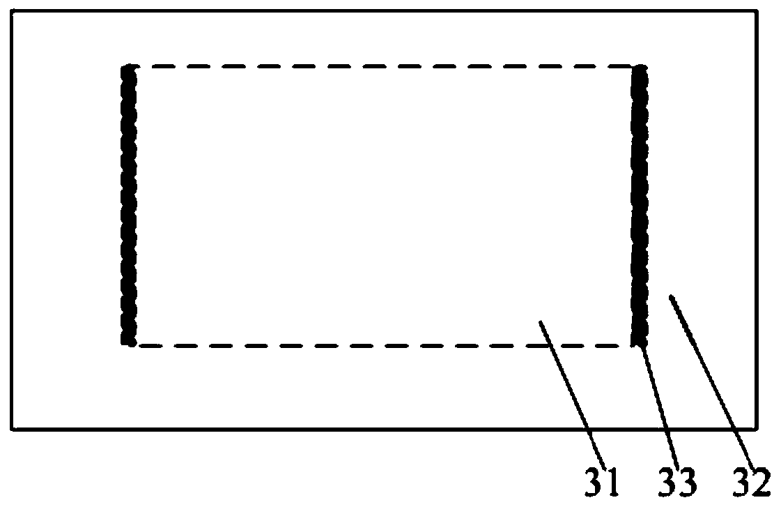
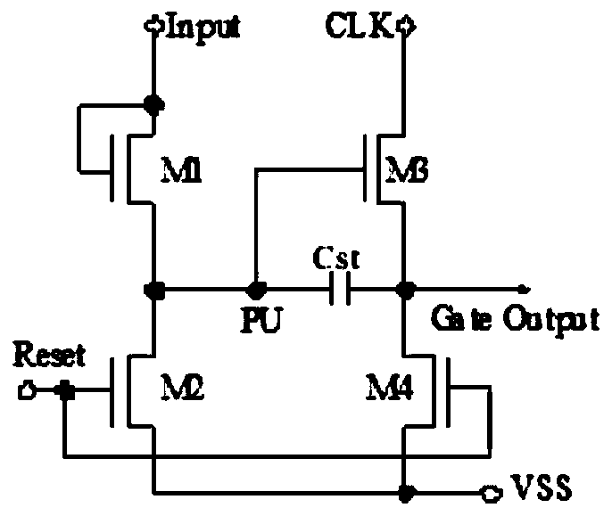
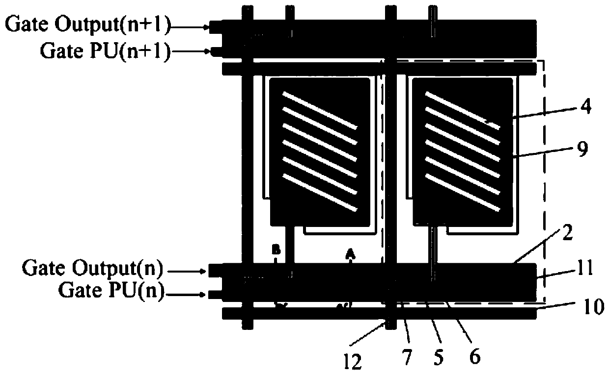
[0046] The pixel structure of a general display product includes a Gate line for controlling the opening of a Thin Film Transistor (TFT), a Data line for writing signals, a common electrode, and a pixel electrode. Based on the TFT LCD display, the present invention takes ADS (Advanced Dimension Switch, adv...


PUM


Abstract

The invention provides a display substrate, a preparation method and a display device. The display substrate comprises: a substrate, wherein a plurality of pixel units are limited by grid lines and data lines which are crisscross at one side of the substrate; a grid electrode for receiving a grid electrode driving signal of a corresponding GOA (Gate driven On Array) unit through the grid line of apixel unit row where the grid electrode locates; and an pull-up electrode which is electrically connected with a pull-up node of a GOA unit corresponding to a pixel unit row where the pull-up electrode locates; wherein the pull-up electrode and the grid electrode are separated at least through an insulation layer, an orthographic projection of at least one of the grid electrode and the grid lineon the substrate and an orthographic projection of the pull-up electrode on the substrate have an overlapped part. The preparation method is suitable for preparing the display substrate. According tothe display substrate of the invention, the pull-up electrode is manufactured within an pixel area, so as to form part or whole of a storage capacitance of a GOA circuit with the grid electrode / grid lines in the pixel area, thereby effectively reducing space occupation of the GOA circuit in a non-display area, and facilitating realization of the display substrate with a narrow frame.

Description

technical field [0001] The invention relates to the field of display technology, in particular to a display substrate, a preparation method and a display device. Background technique [0002] Generally speaking, for GOA (Gate Driven on Array, gate drive integration on array substrate) circuit products, the structure for realizing the gate drive function is arranged in the non-display area of ​​the display panel. like figure 1 As shown, the display panel includes a display area 31 and a non-display area located at the periphery of the display area, wherein the GOA circuit can be arranged on opposite sides of the display area (double-sided driving), figure 1 A GOA region 32 is shown in the non-display region, with a capacitive region 33 therein. In addition, the GOA circuit can also be set on one side of the display area (unilateral drive). GOA technology helps to achieve narrow bezels, but while realizing extremely narrow bezels of display products, the wiring space of the...

Claims


Application Information

Patent Timeline
IPC IPC(8): G02F1/1343G02F1/1362G02F1/1333G09G3/36
CPCG02F1/1343G02F1/1362G02F1/1333G09G3/3674
Inventor 杜瑞芳沈梦钱海蛟马小叶
Owner BOE TECH GRP CO LTD
Why Eureka
Try Eureka