Display panel, manufacturing method of display panel and display device

A technology for display panels and substrate substrates, which is applied in the field of display panels and display devices, and can solve problems such as poor display uniformity of OLED devices

Active Publication Date: 2020-02-04
WUHAN TIANMA MICRO ELECTRONICS CO LTD
View PDF4 Cites 17 Cited by
  • Summary
  • Abstract
  • Description
  • Claims
  • Application Information

AI Technical Summary

Problems solved by technology

[0004] The embodiment of the present invention provides a display panel, its manufacturing method and display device, which are used to alleviate the display uniformity of the OLED device caused by the thin film thickness of the cathode poor problem

Method used


Image

  • Display panel, manufacturing method of display panel and display device
  • Display panel, manufacturing method of display panel and display device
  • Display panel, manufacturing method of display panel and display device

Examples


Embodiment Construction

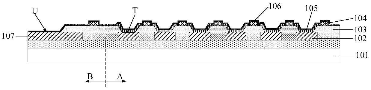
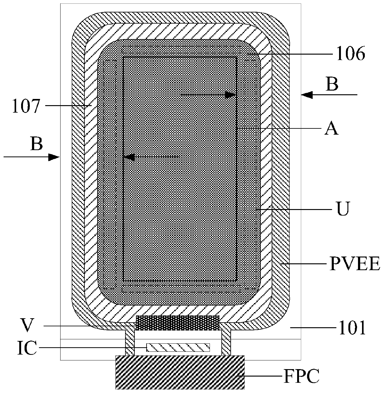
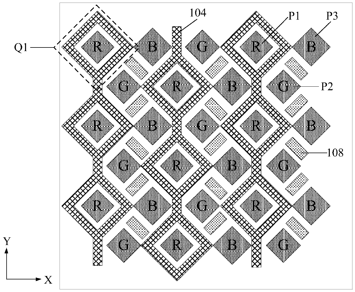
[0032] Aiming at the problem of poor display uniformity of the OLED device caused by the thin film thickness of the cathode existing in the prior art, embodiments of the present invention provide a display panel, a manufacturing method thereof, and a display device.

[0033] In order to make the above objects, features and advantages of the present invention more comprehensible, the present invention will be further described below in conjunction with the accompanying drawings and embodiments. Example embodiments may, however, be embodied in many forms and should not be construed as limited to the embodiments set forth herein; rather, these embodiments are provided so that this disclosure will be thorough and complete, and will fully convey the concept of example embodiments to those skilled in the art. The same reference numerals denote the same or similar structures in the drawings, and thus their repeated descriptions will be omitted. The words expressing position and dire...


PUM


Abstract

The invention discloses a display panel, a manufacturing method of the display panel and a display device. The display panel comprises an underlayer substrate, a plurality of first electrodes, a pixeldefining layer, a connecting metal layer, an organic light-emitting function layer and a second electrode, wherein the pixel defining layer and the first electrodes are located on the same side of the underlayer substrate, and the pixel defining layer comprises a plurality of openings for exposing the first electrodes respectively; the connecting metal layer is located on the side, which deviatesfrom the underlayer substrate, of the pixel defining layer, and the orthographic projection of a pattern of the connecting metal layer on the underlayer substrate at least half surrounds the openings; the second electrode is located on the sides, which deviate from the underlayer substrate, of the organic light-emitting function layer and the pixel defining layer, and the orthographic projectionof the second electrode on the underlayer substrate covers the orthographic projection of the pixel defining layer and the orthographic projection of the first electrodes on the underlayer substrate;and the second electrode is electrically connected with the connecting metal layer. Due to the fact that the connecting metal layer is connected with the second electrode in parallel, the in-plane resistance of the second electrode is reduced, the voltage drop in the display area is reduced, the voltage distribution in the display area is more uniform, and the display uniformity of the display panel is improved.

Description

technical field [0001] The invention relates to the field of display technology, in particular to a display panel, a manufacturing method and a display device. Background technique [0002] Organic Light-Emitting Diode (OLED) has the advantages of self-luminescence, fast response, wide viewing angle, high brightness, bright color, light and thin, etc., and is considered to be the next generation display technology. OLED devices have two light emitting methods: bottom emission and top emission. Compared with top emission OLED devices, top emission OLED devices have better resolution and color saturation, and have high luminous efficiency, wide color gamut and long life. [0003] In a top-emitting OLED device, the cathode should have high transmittance and strong conductivity. To ensure that the cathode has a high transmittance, the film thickness of the cathode needs to be very thin. However, the thinner the film thickness of the cathode The larger the resistance value will ...

Claims


Application Information

Patent Timeline
Patent Type & Authority Applications(China)
IPC IPC(8): H01L27/32H01L51/52H01L51/56
CPCH10K59/1315H10K50/805H10K59/1201H10K71/00H10K59/352H10K59/353H10K50/824H10K50/852H10K71/166
Inventor 辛宇韩立静陈娴
Owner WUHAN TIANMA MICRO ELECTRONICS CO LTD
Why Eureka
Try Eureka