Eureka AIR delivers breakthrough ideas for toughest innovation challenges, trusted by R&D personnel around the world.

External etching compensation method for precision circuit

A compensation method and external compensation technology, applied in chemical/electrolytic methods to remove conductive materials, printed circuits, printed circuit manufacturing, etc., can solve problems such as difficult, complex, and complex operations, and achieve simple compensation rules and convenient design , The effect of low design work difficulty

Pending Publication Date: 2020-02-04
江苏上达半导体有限公司
View PDF6 Cites 2 Cited by
  • Summary
  • Abstract
  • Description
  • Claims
  • Application Information

AI Technical Summary

Problems solved by technology

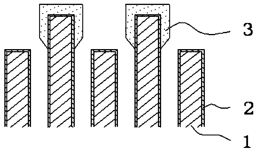
Since the front ends of long lines of different products have different degrees of space, or the front ends of long lines in different regions of the same product have different degrees of space, it is necessary to design multiple corresponding special compensation rules according to the degree of space, and the operation is very complicated.
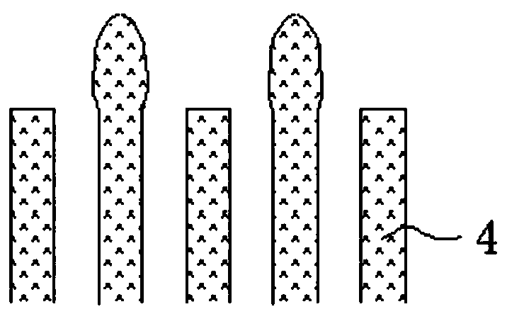
[0005] Additionally, if figure 1 The special compensation of the regular figure as shown, because the special compensation part is strongly corroded by the open area, the result will be as follows figure 2 As shown, the difference between the actual line 4 after etching off the special compensation area and the ideal line 1 is obvious
This method is more complicated and difficult unless the circuit is compensated with complex shapes and then adjusted the shape and size of the compensation according to the etching effect.

Method used


Image

  • External etching compensation method for precision circuit
  • External etching compensation method for precision circuit
  • External etching compensation method for precision circuit

Examples


Embodiment Construction

[0021] In order to make the object, technical solution and advantages of the present invention clearer, the present invention will be further described in detail below. However, it should be understood that the specific embodiments described here are only used to explain the present invention, and are not intended to limit the scope of the present invention.

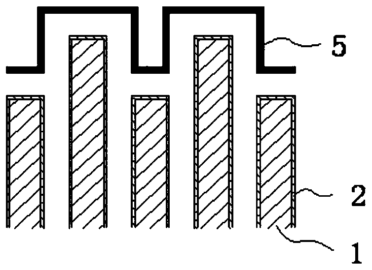
[0022] An external etching compensation method for precision circuits. Firstly, a uniform blank area is formed around the circuit. During etching, the density of the area where the circuit is located is the same, and the etching effect is consistent. After etching, a uniform circuit is obtained.

[0023] Specifically, such as image 3 As shown, when there are long and short lines arranged in a staggered manner, first perform conventional compensation 2 on the entire line, and then perform external compensation 15 at a certain distance from the front end of each line and the side of the long line, and obtain a uniform lin...


PUM


Abstract

The invention discloses an external etching compensation method for a precision circuit, which is characterized in that a uniform blank area is formed around the circuit, and a uniform circuit is obtained after etching. According to the invention, a regular external compensation pattern is designed around the circuit so as to form the same density around the circuit, the liquid medicine exchange speed is the same, the size difference of different areas and different types of circuit patterns can be eliminated, the same etching effect is finally achieved, and a uniform circuit is obtained. Besides, the adopted external compensation pattern is a regular pattern, so that the design work difficulty is low, the compensation rule is simple, and the design is convenient. In addition, the externalcompensation pattern is designed to be narrow, so that the external compensation pattern is laterally etched off in the etching process, and other special treatment is not needed.

Description

technical field [0001] The invention relates to an external etching compensation method for precision circuits. Background technique [0002] Affected by the pin arrangement of the IC chip, the front end of the line is not in a straight line, but arranged in a staggered length. The density at the front end of the long pins is small, which is an open area; the density at the short pins is relatively high, which is a dense area. [0003] During etching, the density of circuit board distribution will lead to differences in the exchange speed of liquid medicine. In the open area, the liquid medicine is not hindered, the exchange is fast, and the amount of etching is large. In dense areas, due to the small gap between the lines, the liquid medicine exchange Slow, the amount of etching is small, so the etching is uneven, and the circuit board forms different etching effects in different areas. The conventional etching compensation method is difficult to meet the line accuracy re...

Claims


Application Information

Patent Timeline
Patent Type & Authority Applications(China)
IPC IPC(8): H05K3/06
CPCH05K3/068
Inventor 方磊王健孙彬沈洪李晓华
Owner 江苏上达半导体有限公司
Why Eureka
Eureka Blog
Learn More