A mechanically connected conduction-cooled semiconductor laser stack package structure

A technology of conduction cooling and mechanical connection, which is applied in the direction of semiconductor laser devices, semiconductor lasers, laser devices, etc., and can solve the problem that the bar affects the output power and output beam of the laser, the laser chip of the electrode connection block cannot be replaced, and the semiconductor laser device can no longer be used. and other problems to achieve the effect of avoiding welding voids, avoiding complex shape and structure, and reducing the risk of cracking

Active Publication Date: 2017-02-08
FOCUSLIGHT TECH
View PDF10 Cites 1 Cited by
  • Summary
  • Abstract
  • Description
  • Claims
  • Application Information

AI Technical Summary

Problems solved by technology

[0002] At present, the existing semiconductor laser packaging is generally to weld the laser chip on the heat sink, and solder the electrode connection block to the heat sink. If the laser chip is damaged or the electrode is connected to the semiconductor laser packaged in this way, If the block is damaged, the entire semiconductor laser device will no longer be usable, and the electrode connection block or laser chip cannot be replaced
In addition, there are many parts, the preparation process is difficult, and the yield rate is low, which also leads to relatively low reliability and long-term life of the product
[0003] For conduction-cooled high-power semiconductor laser arrays and liquid-cooled horizontal array high-power semiconductor laser arrays (a high-power semiconductor laser, Chinese utility model patent, publication number CN101071933, publication date November 14, 2007), due to the horizontal array structure It is welded together by multiple bars. Once a bar is burned, short-circuited or not working properly, it will directly affect the output power and output beam of the entire laser, so it cannot be replaced
At the same time, the undamaged bars in the array will be wasted, so the manufacturing cost is very high

Method used


Image

  • A mechanically connected conduction-cooled semiconductor laser stack package structure
  • A mechanically connected conduction-cooled semiconductor laser stack package structure
  • A mechanically connected conduction-cooled semiconductor laser stack package structure

Examples


Embodiment Construction

[0033] The following embodiment is the best embodiment of the present invention, but those skilled in the art should know that this embodiment does not limit the present invention after reading the foregoing solutions.

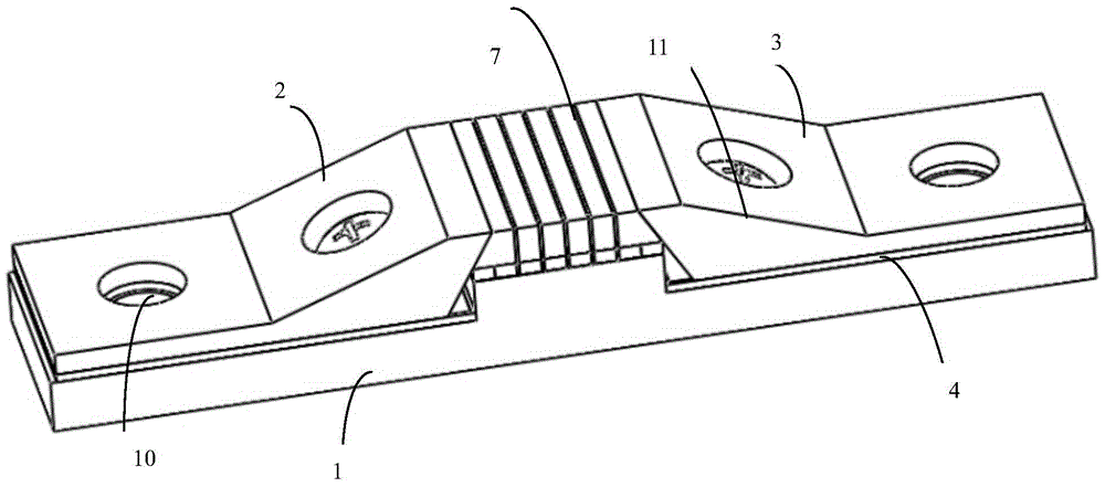
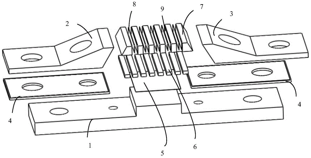
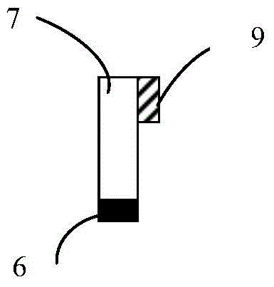
[0034] The conduction cooling type semiconductor laser array of the present embodiment, such as figure 1 and figure 2 The shown includes a basic heat sink 1, a positive electrode connection block 2, a negative electrode connection block 3 (the crimping part is wedge-shaped) and a laser stack mainly composed of a plurality of chip modules. The positive electrode connection block 2 and the negative electrode connection block 3 are installed on the basic heat sink through the insulating sheet 4, and the laser array is installed on the basic heat sink through the insulating structure, and the core insulating structure 5 also has heat conduction and stress release properties; the chip module mainly It includes a substrate 7 and a laser chip 9 welded to the substr...


PUM


Abstract

The invention provides a mechanical connection conducting cooling type semiconductor laser unit stack packaging structure which is used for improving the reliability of a product and prolonging the service life of the product. On an insulation structure, a laser unit stack is located in the middle, a positive electrode connecting block and a negative electrode connecting block are located on the two sides of the laser unit stack, the positive electrode connecting block and the negative electrode connecting block are fixedly connected with a basic heat sink in the mode that fastening screws obliquely penetrate through the insulation structure downwards, the opposite inner side faces of the positive electrode connecting block and the negative electrode connecting block are both slopes, the two slopes are closed downwards overall, and the outer side faces at the two ends of the whole laser unit stack are also slopes which are matched with the two slopes respectively, so that under the screwing effect of the fastening screws arranged obliquely downwards, all chip modules are pressed to the middle and downwards through the positive electrode connecting block and the negative electrode connecting block, and therefore the mechanical connection conducting cooling type semiconductor laser unit stack packaging structure is finally acquired.

Description

technical field [0001] The invention belongs to the field of semiconductor laser packaging, and relates to a conduction cooling type semiconductor laser stack packaging structure. Background technique [0002] At present, the existing semiconductor laser packaging is generally to weld the laser chip on the heat sink, and solder the electrode connection block to the heat sink. If the laser chip is damaged or the electrode is connected to the semiconductor laser packaged in this way, If the block is damaged, the entire semiconductor laser device will no longer be usable, and the electrode connection block or laser chip cannot be replaced. In addition, there are many parts, the preparation process is difficult, and the yield rate is low, which also leads to relatively low reliability and long-term life of the product. [0003] For conduction-cooled high-power semiconductor laser arrays and liquid-cooled horizontal array high-power semiconductor laser arrays (a high-power semic...

Claims


Application Information

Patent Timeline
Patent Type & Authority Patents(China)
IPC IPC(8): H01S5/022H01S5/024H01S5/40
Inventor 王警卫侯栋刘兴胜
Owner FOCUSLIGHT TECH
Why Eureka
Try Eureka