Optical semiconductor lighting apparatus

a technology of optical semiconductors and lighting apparatuses, applied in lighting and heating apparatus, lighting support devices, light source combinations, etc., can solve the problems of relative dark area generated between the lenses, subjected to optical loss, moisture or other foreign matter is likely to enter the light emitting module, etc., to improve durability, convenient overhaul and repair, and convenient assembly and disassembly of the lighting apparatus

Inactive Publication Date: 2013-04-11
POSCO LED
View PDF4 Cites 52 Cited by
  • Summary
  • Abstract
  • Description
  • Claims
  • Application Information

AI Technical Summary

Benefits of technology

[0065]First, the lighting apparatus includes a housing, which can be divided into a plurality of detachable components and surrounds a light emitting module including an optical semiconductor device, thereby enabling convenient assembly and disassembly of the lighting apparatus while improving durability.
[0066]In addition, the respective components of the housing may be separated from each other, whereby an operator can conveniently overhaul and repair the lighting apparatus when the lighting apparatus fails.
[0067]Further, the lighting apparatus includes a sealing member between the optical cover and a heat sink, thereby providing a waterproof and air-tight structure.
[0068]Further, the optical cover, the optical semiconductor...

Problems solved by technology

In the conventional lighting apparatus, however, a relatively dark area can be generated between the lenses.
In addition, light emitted from the optical semiconductor devices passes through the optical cover after passing through the lenses, and is thus subjected to optical loss.
Further, moisture or other foreign matter is likely to enter the light emitting module through a gap between the optical cover and the heat sink.
In this case, the lighting apparatus needs a complicated wire connection structure to supply power from a power source to the light emitting modules through a main power wire.
At this time, such a complicated wire connection structure increases manufacturing costs while reducing ope...

Method used


Image

  • Optical semiconductor lighting apparatus
  • Optical semiconductor lighting apparatus
  • Optical semiconductor lighting apparatus

Examples


Embodiment Construction

[0108]Next, embodiments of the present invention will be described in detail with reference to the accompanying drawings.

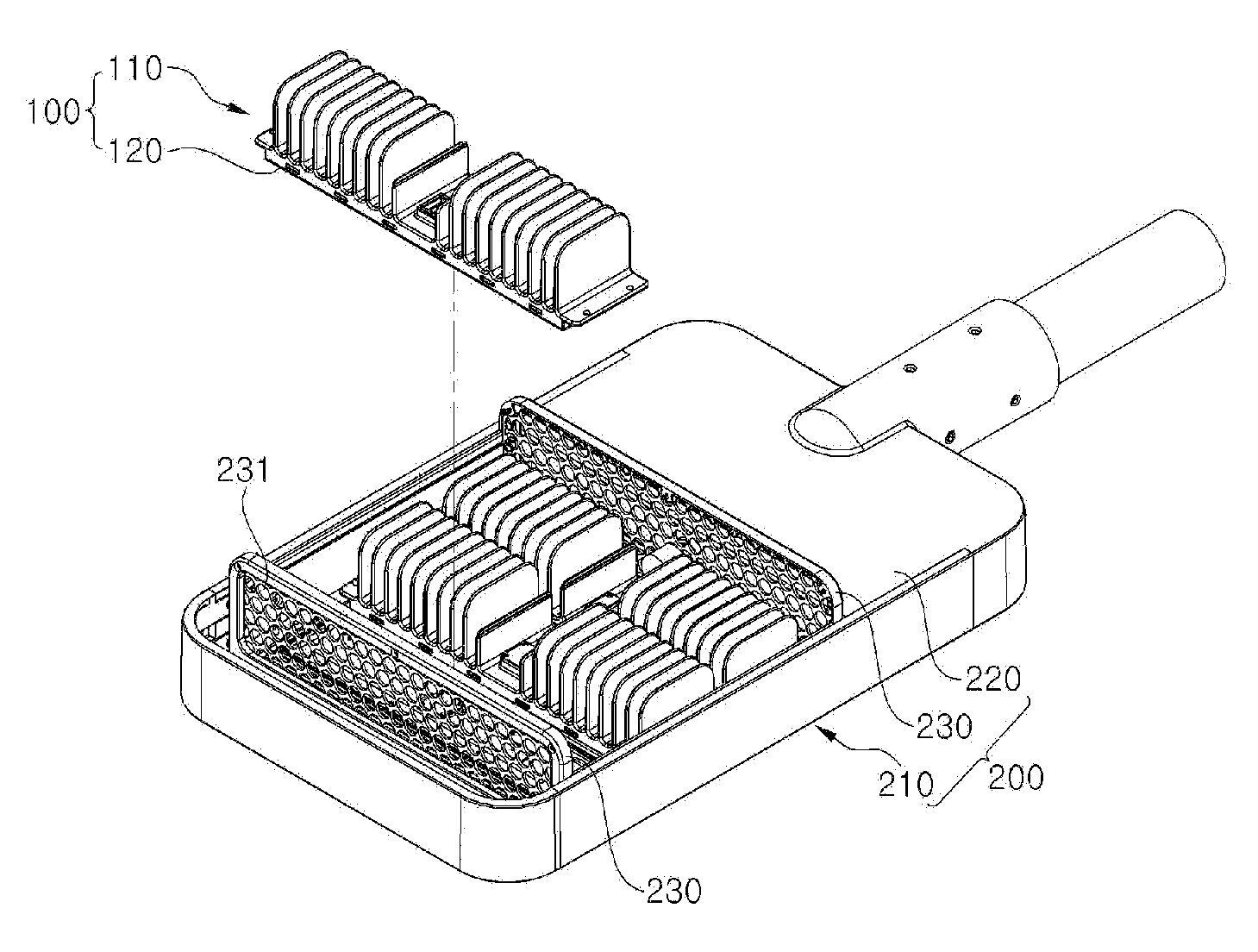
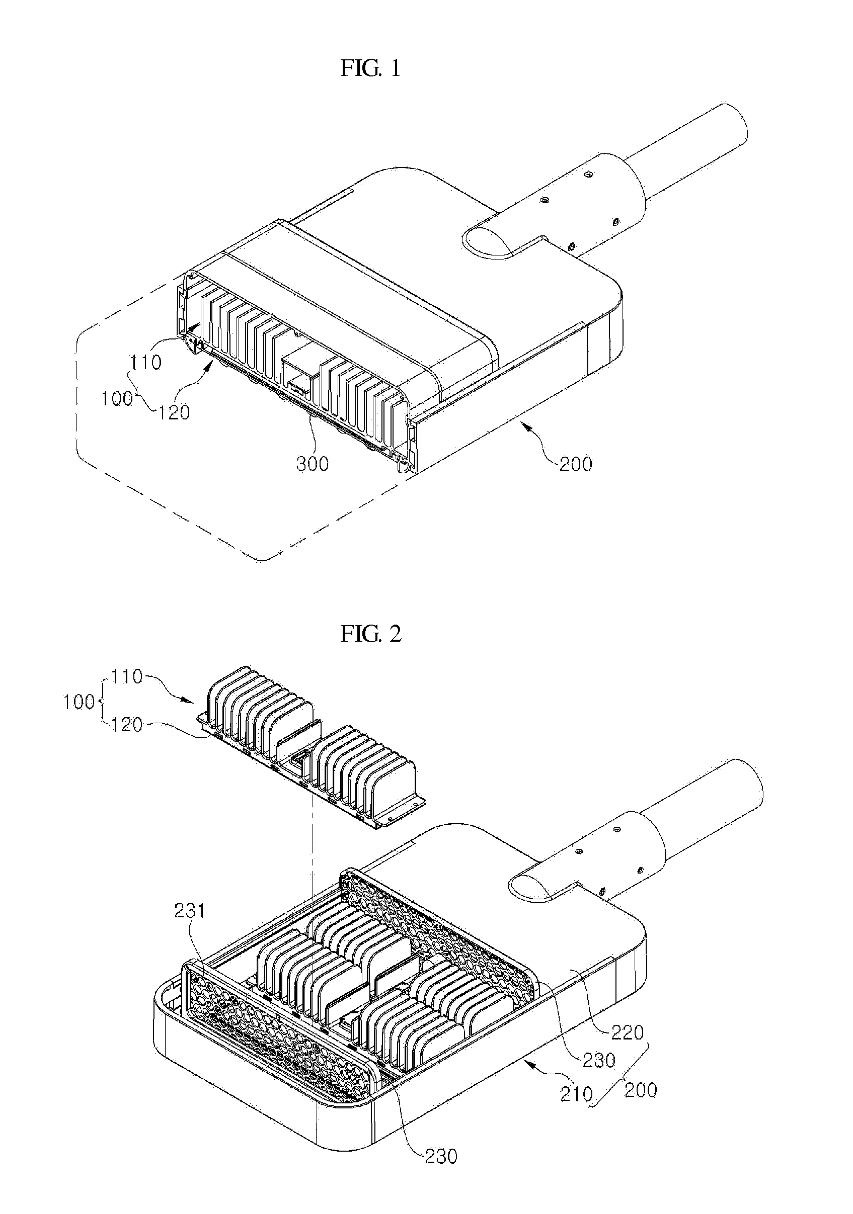
[0109]FIG. 1 is a partially cut-away perspective view of an optical semiconductor lighting apparatus in accordance with one embodiment of the present invention, and FIG. 2 is an exploded perspective view of the optical semiconductor lighting apparatus in accordance with the embodiment of the present invention, in which a light emitting module is separated from a housing of the lighting apparatus.

[0110]As shown in the drawings, the lighting apparatus according to this embodiment includes a housing 200 which receives a light emitting module 100 therein. The light emitting module 100 includes a heat sink 110, which includes optical semiconductor devices 150 disposed thereon, and an optical cover 120 coupled to the heat sink 110.

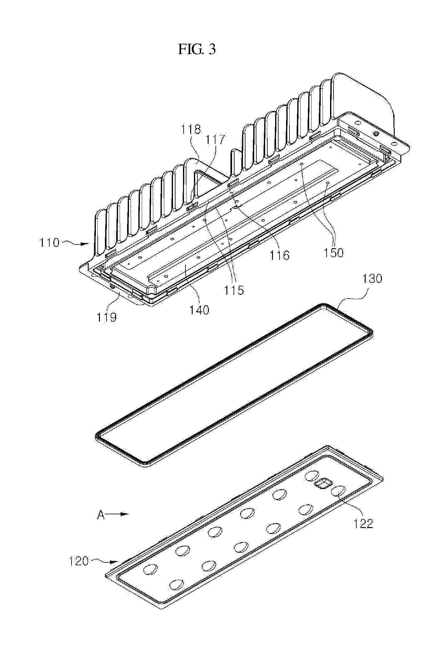
[0111]In FIG. 1, reference numeral 140 denotes a printed circuit board.

[0112]Referring to FIG. 2, the housing 200 includes a support frame 22...


PUM

PropertyMeasurementUnit
Lengthaaaaaaaaaa
Widthaaaaaaaaaa
Circumferenceaaaaaaaaaa

Abstract

An optical semiconductor lighting apparatus includes a heat sink including a heat dissipation base and a plurality of heat dissipation fins formed on a lower surface of the heat dissipation base; an optical semiconductor device placed on the heat dissipation base; and an optical cover coupled to an upper side of the heat sink to cover the optical semiconductor device. The heat dissipation base is formed with an air flow hole through which upper ends of the heat dissipation fins are exposed.

Description

CROSS REFERENCE TO RELATED APPLICATIONS[0001]This application claims priority from and the benefit of Korean Patent Application No. 10-2011-0103826, filed on Oct. 11, 2011; No. 10-2011-0116740, filed on Nov. 10, 2011; No. 10-2012-0026853, filed on Mar. 16, 2012; and No. 10-2012-0054719, filed on May 23, 2012, all of which are hereby incorporated by reference for all purposes as if fully set forth herein.BACKGROUND[0002]1. Technical Field[0003]The present invention relates to an optical semiconductor lighting apparatus.[0004]2. Description of the Related Art[0005]Optical semiconductor devices such as light emitting diodes (LEDs) have is attracted increasing attention due to excellent advantages such as low power consumption, long lifespan, high durability, and excellent brightness, as compared with incandescent lamps or fluorescent lamps.[0006]In particular, an optical semiconductor device is free from toxic or environmentally unfriendly substances such as mercury injected into a gla...

Claims


Application Information

Patent Timeline
IPC IPC(8): F21V29/00F21V5/04F21V21/00
CPCF21S2/005F21V29/83F21V3/0445F21V5/007F21V5/02F21V17/164F21V23/006F21V23/06F21W2131/10F21Y2101/02F21Y2103/003F21Y2105/001F21V29/004F21V29/006F21V31/005F21V29/2206F21S4/008F21V29/507F21V29/74F21V29/763F21V29/777F21V3/0436F21Y2113/00F21V29/506F21V29/51F21S4/28F21Y2103/10F21Y2105/10F21Y2115/10F21V3/062F21V3/0625
Inventor YUN, KYUNG MINKIM, MIN SUKIM, JUNG HWAKIM, DONG SOOKIM, KYOO SEOK
Owner POSCO LED
Why Eureka
Try Eureka