
Touch electrode layer and touch display device

A technology of touch electrodes and electrodes, which is applied in the fields of electrical digital data processing, instruments, calculations, etc., can solve the problems of lower touch sensitivity, large RC delay, small capacitance change, etc., and achieve improved resolution and accuracy, mutual Capacitance and electric field distribution is uniform and the effect of improving the mutual capacitance value

Active Publication Date: 2020-02-07
WUHAN CHINA STAR OPTOELECTRONICS SEMICON DISPLAY TECH CO LTD
View PDF7 Cites 13 Cited by
  • Summary
  • Abstract
  • Description
  • Claims
  • Application Information

AI Technical Summary

Problems solved by technology

At present, for flexible active-matrix organic light-emitting diode (AMOLED) displays, the touch electrode patterns usually need to be directly fabricated on the upper surface of the thin-film packaging layer. However, due to the thin packaging layer (usually Thickness<10um), so the distance between the touch electrode and the cathode is small, resulting in a large parasitic capacitance between the driving electrode (TX) / sensing electrode (RX) and the cathode, resulting in a large RC delay and reducing the touch Sensitivity
And the current flexible AMOLED display, and the material of the touch electrode is usually a hollow metal grid material, its conductive area is compared with the traditional full-surface transparent ITO material touch electrode, its actual effective conductive electrode area is smaller, so the touch The mutual capacitance inductance between the electrodes TX and RX is very small, resulting in a smaller capacitance change when touched by a finger, which is not easily detected by the touch chip

Method used


Image

  • Touch electrode layer and touch display device
  • Touch electrode layer and touch display device
  • Touch electrode layer and touch display device

Examples


Embodiment 1

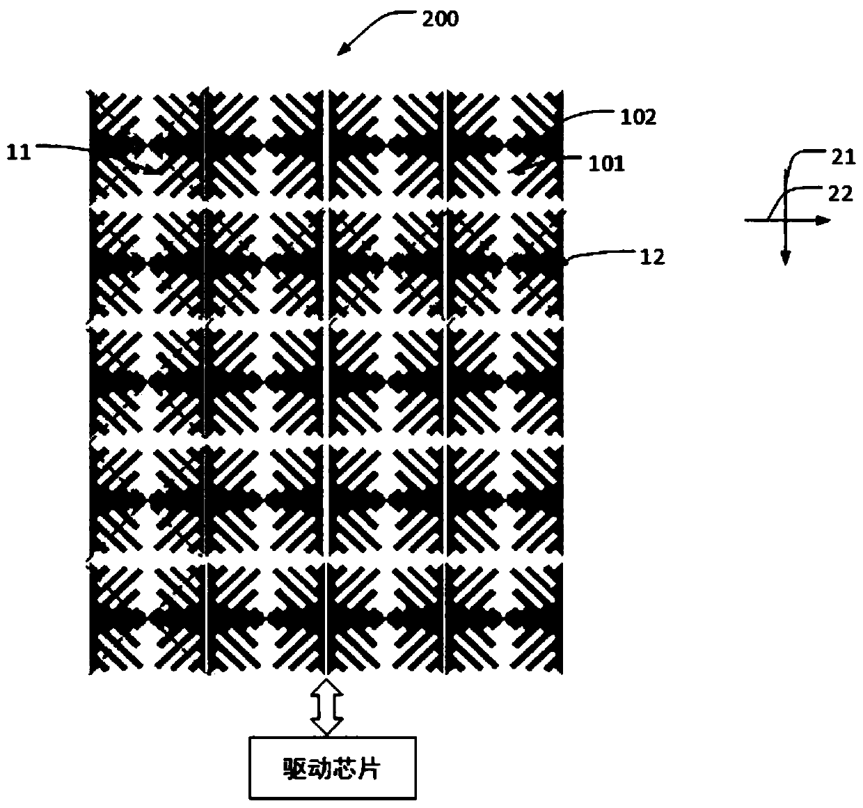
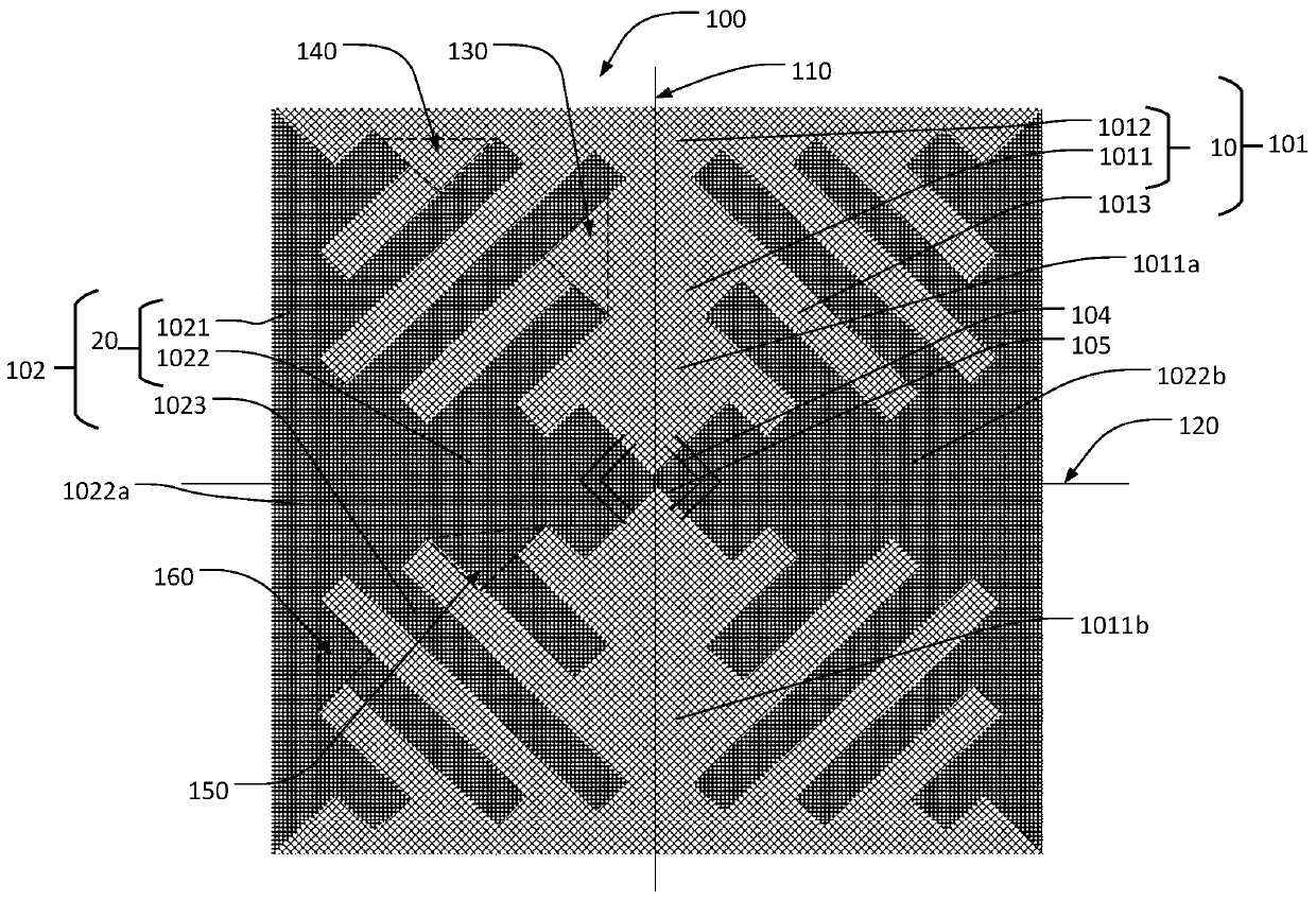
[0049] like figure 1 As shown, the present invention provides a touch electrode layer 200. In Embodiment 1, it includes a plurality of first electrode chains 11 arranged along the first direction 21, and each first electrode chain includes a plurality of first electrode chains 11 electrically connected to each other. An electrode 101; a plurality of second electrode chains 12 arranged along the second direction 22, each second electrode chain 12 comprising a plurality of second electrodes 102 electrically connected to each other, each first electrode chain 11 and each second electrode chain The electrode chains 12 are insulated from each other. The first direction 21 is perpendicular to the second direction 22 . The first electrode chain 11 is figure 1 The marked longitudinal dotted rhombus box indicates that the second electrode chain 12 is figure 1 Marked horizontal rhombus dashed box.

[0050] Each first electrode 101 and the second electrode 102 corresponding to each f...

Embodiment 2

[0085] like Figure 5 As shown, the present invention provides the touch electrode layer 200a of Embodiment 2. The difference between Embodiment 2 and Embodiment 1 is that the first middle part between the first electrode branch 1013a and the first electrode 10a trunk The shape of 130a is a right-angled trapezoid, and the height of the right-angled trapezoid is perpendicular to the first electrode trunk 10a.

[0086] The shape of the second intermediate portion 140a between the second electrode branch 1014a and the second electrode 20a is also a right-angled trapezoid, and the height of the right-angled trapezoid is perpendicular to the second electrode trunk 20a.

Embodiment 3

[0088] like Image 6 As shown, the present invention provides the touch electrode layer 200b of Embodiment 3. The difference between Embodiment 3 and Embodiment 2 is that the first electrode branch 1013b has at least one electrode protrusion 1014b, and the electrode protrusion 1014b is vertical on the first electrode branch 1013b. The second electrode branch 1023b has a groove 1024b, and the electrode protrusion 1013b is locked into the groove 1024b.

[0089] The electrode protrusion 1014b can further increase the Tx / Rx adjacent interface coupling area to increase the variation ΔCm of the mutual capacitance signal when touched by a finger, thereby effectively improving the touch sensitivity.


PUM


Abstract

The invention provides a touch electrode layer and a touch display device. The touch electrode layer is provided with a first electrode and a second electrode, the first electrode is provided with a first electrode trunk and a plurality of first electrode branches which are obliquely arranged along the first electrode trunk; the second electrode is provided with a second electrode trunk and a plurality of second electrode branches obliquely arranged along the second electrode trunk, the first electrode and the second electrode are both arranged to be of a symmetrical structure, and the inclination angles of the first electrode branches and the second electrode branches are the same. In the touch electrode unit, the first electrodes and the second electrodes are almost the same in shape andsize, and the first electrode branches and the second electrode branches which are arranged in a crossed mode are also almost the same in shape and size. The mutual capacitance value between the touch driving electrodes and the touch sensing electrodes can be effectively improved, meanwhile, a mutual capacitance electric field in the whole touch screen structure is distributed more evenly, and the resolution and accuracy of touch position detection can be better improved.

Description

technical field [0001] The present invention relates to the field of touch display, in particular to a touch electrode layer and a touch display device. Background technique [0002] Capacitive touch screens are widely used in various electronic interactive scene devices due to their high durability, long life, and support for multi-touch functions. Capacitive touch screen detects the specific position touched by the finger by detecting the change of capacitance at the position touched by the finger. Therefore, when the amount of capacitance change caused by touch is small, the traditional capacitive touch screen may not be able to accurately detect whether there is a touch input. [0003] Since the structural design of the touch screen is a very important factor for detecting the capacitance change, it is very necessary to develop a touch screen design capable of detecting a small capacitance change. At present, for flexible active-matrix organic light-emitting diode (AMO...

Claims


Application Information

Patent Timeline
Patent Type & Authority Applications(China)
IPC IPC(8): G06F3/044G06F3/041
CPCG06F3/044G06F3/0412G06F2203/04111G06F3/0448G06F3/0443G06F3/0446G06F3/0445
Inventor 叶剑
Owner WUHAN CHINA STAR OPTOELECTRONICS SEMICON DISPLAY TECH CO LTD
Learn More