Touch control assembly and touch display device

A technology of a touch display device and a touch component, which is applied in the direction of instruments, electrical digital data processing, and the input/output process of data processing, etc., and can solve the problems that are not conducive to the improvement of touch reporting rate, increase of touch scanning time, Problems such as the decrease of the touch report rate, to achieve the effect of increasing the report rate, reducing the resistance and capacity load, and reducing the time

Active Publication Date: 2020-10-13
SHENZHEN CHINA STAR OPTOELECTRONICS SEMICON DISPLAY TECH CO LTD
View PDF10 Cites 3 Cited by
  • Summary
  • Abstract
  • Description
  • Claims
  • Application Information

AI Technical Summary

Problems solved by technology

Since the driving electrode Tx and the sensing electrode Rx are diamond-shaped, the impedance load of the driving electrode Tx and the sensing electrode Rx is relatively large, resulting in an increase in the scanning time of the touch control, resulting in a decrease in the report rate of the touch control, which is not conducive to satisfying the touch report point demand for rate increases
[0004] Therefore, it is necessary to propose a technical solution to solve the problem that the touch report rate is reduced due to the large impedance load when the driving electrodes and sensing electrodes are diamond-shaped.

Method used


Image

  • Touch control assembly and touch display device
  • Touch control assembly and touch display device
  • Touch control assembly and touch display device

Examples


Embodiment Construction

[0051] The technical solutions in the embodiments of the present application will be clearly and completely described below in conjunction with the drawings in the embodiments of the present application. Apparently, the described embodiments are only some of the embodiments of this application, not all of them. Based on the embodiments in this application, all other embodiments obtained by those skilled in the art without making creative efforts belong to the scope of protection of this application.

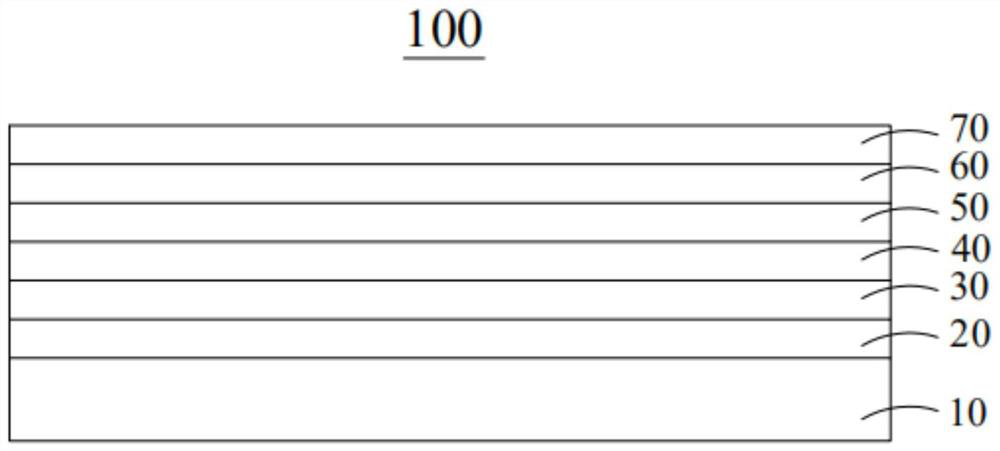
[0052] The touch display device of the present application includes a display panel and a touch component, and the touch component is located on the light emitting side of the display panel. The display panel includes a plurality of sub-pixels. The touch component includes a touch layer. The display panel can be an organic light emitting diode display panel, or a liquid crystal display panel. For ease of description, this embodiment is described by taking the display panel as ...


PUM

PropertyMeasurementUnit
capacitanceaaaaaaaaaa
thicknessaaaaaaaaaa

Abstract

The invention provides a touch control assembly and a touch control display device. The touch control assembly comprises a touch control layer; the touch control layer comprises a plurality of touch control units; each touch control unit comprises a first electrode arranged along a first direction, and a second electrode arranged in the second direction, wherein the first electrode is electricallyinsulated from the second electrode. At the position close to the intersection of the first electrode and the second electrode, the first electrode comprises at least one concave part, and the secondelectrode comprises at least one convex part matched with the concave part. The concave part is arranged on each first electrode, and the convex part is arranged on each second electrode; therefore,the impedance of the first electrode at the position close to the intersection of the first electrode and the second electrode is not increased, and the impedance of the second electrode at the position close to the intersection of the first electrode and the second electrode is reduced, so that the resistance-capacitance load of the second electrode is reduced, the scanning time of the touch display device is shortened, and the point reporting rate is increased.

Description

technical field [0001] The present application relates to the field of touch technology, in particular to a touch component and a touch display device. Background technique [0002] Capacitive touch screens are widely used in various electronic interactive scene devices due to their high durability, long life, and support for multi-touch functions. The capacitive touch screen detects the specific position touched by the finger by detecting the change of capacitance at the position touched by the finger. [0003] like figure 1 As shown, it is a schematic diagram of the touch electrode of the traditional flexible active matrix organic light emitting diode (Active Metrix OrganicLight Emitting Diode, AMOLED) touch oncell display screen. The touch electrode includes a driving electrode Tx and a sensing electrode Rx. The driving electrode Tx and the sensing electrode Rx are arranged on the same layer and are insulated from each other. The driving electrode Tx and the sensing ele...

Claims


Application Information

Patent Timeline
Patent Type & Authority Applications(China)
IPC IPC(8): G06F3/041G06F3/044
CPCG06F3/0412G06F3/0446G06F2203/04112G06F3/0448G06F2203/04111
Inventor 叶剑
Owner SHENZHEN CHINA STAR OPTOELECTRONICS SEMICON DISPLAY TECH CO LTD
Why Eureka
Try Eureka