A test method for field of view splicing accuracy of large field of view area array devices

A field of view splicing and precision testing technology, applied in the field of aerospace optical remote sensors, can solve the problems of low installation and adjustment accuracy, difficult engineering realization, etc., and achieve the effect of strong operability and small environmental interference factors.

Active Publication Date: 2021-08-10
BEIJING RES INST OF SPATIAL MECHANICAL & ELECTRICAL TECH
View PDF8 Cites 0 Cited by
  • Summary
  • Abstract
  • Description
  • Claims
  • Application Information

AI Technical Summary

Problems solved by technology

[0005] The technical problem solved by the present invention is: to overcome the deficiencies of the prior art, to propose a method for testing the splicing accuracy of the field of view of a large field of view area array device, to realize the splicing of the existing detector's field of view from the perspective of actual assembly and adjustment, and to solve the problems of the prior art Existing problems of low assembly accuracy and difficult engineering realization

Method used


Image

  • A test method for field of view splicing accuracy of large field of view area array devices
  • A test method for field of view splicing accuracy of large field of view area array devices
  • A test method for field of view splicing accuracy of large field of view area array devices

Examples


Embodiment Construction

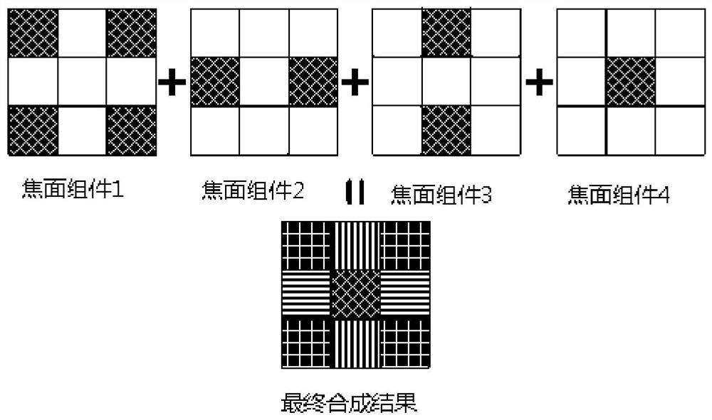
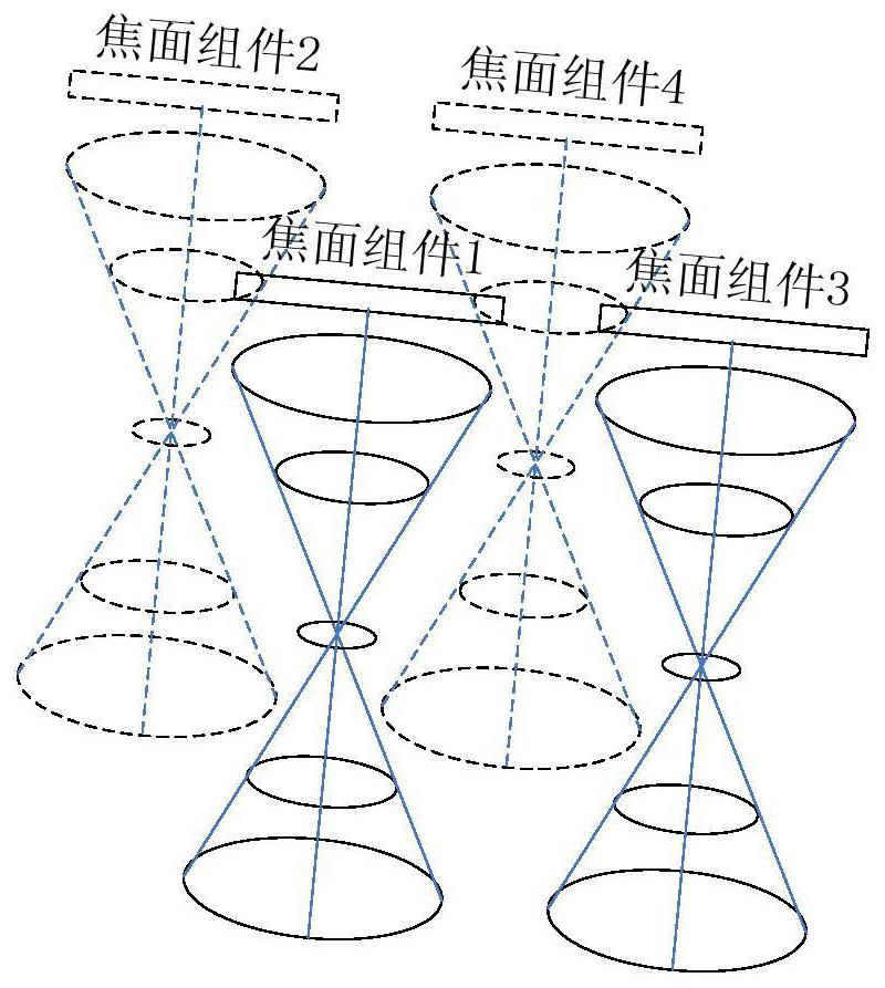
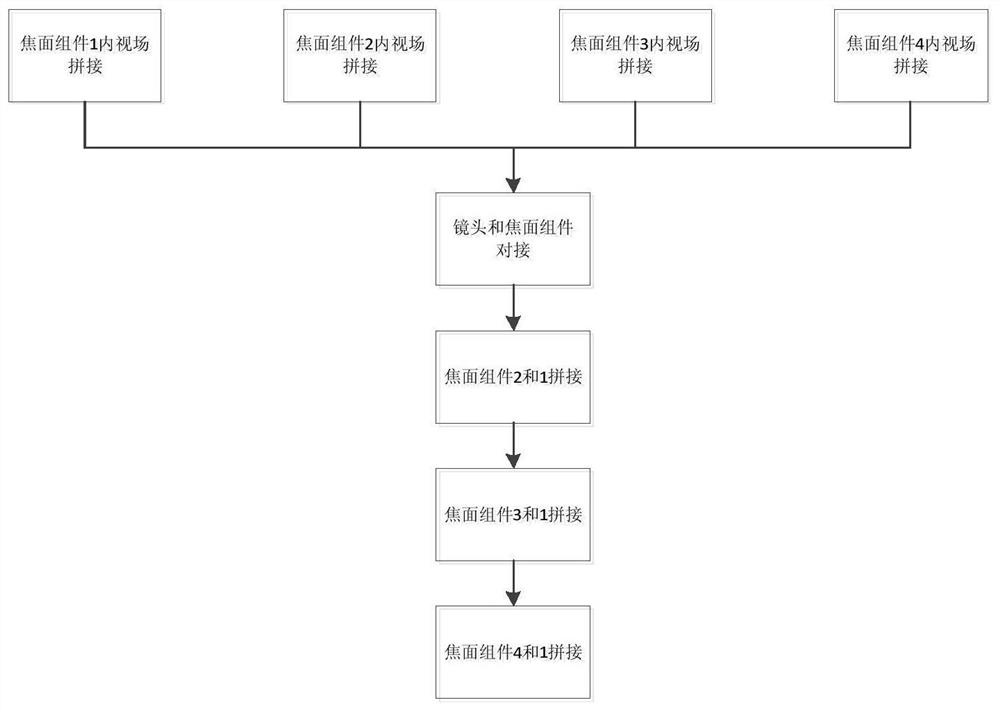
[0052] Set N = 4, M 1 = 4, M 2 = M 3 = 2, M 4 =1. The camera parameters that need field of view stitching are: the entire camera uses 4 sets of optical lenses, and these 4 sets of optical lenses correspond to different numbers of CMOS area array devices with a pixel number of 10k×10k, namely 4, 2, and 2 , 1. Through the mixed stitching method of the inner and outer fields of view, the resulting images are superimposed to achieve 3×3 CMOS digital back stitching, reaching a large format with a total number of pixels of about 30k×30k. The stitching process and the stitching are shown as follows figure 1 shown. The camera optical system and focal plane are composed of figure 2 shown.

[0053] The size of the focal plane of the four groups of lenses is as follows: figure 2 As shown (focal plane 2 and focal plane 3 correspond to the same optical system). In order to ensure the consistency of the optical system as much as possible, the panchromatic optical system correspon...


PUM


Abstract

A method for splicing the field of view of an area array device with a large field of view in the present invention, the steps are as follows: 1) N groups of lenses are set; the number of lenses is N≥2; the number of area array devices contained in the focal plane assembly corresponding to each lens is respectively m N a; M N The value of is greater than or equal to 1; 2) The inner field of view is spliced ​​for the focal plane components corresponding to the N lenses; 3) The lens is connected to the corresponding focal plane component to adjust the direction of the optical axis; 4) The focal plane between the lenses Surface components are used for external field of view stitching. 5) Repeat step 4) to complete the splicing of the outer field of view of the remaining focal plane components until the splicing of the field of view of all area array devices is completed. The splicing method of the invention has strong operability and strong practical value.

Description

technical field [0001] The invention relates to a field-of-view splicing accuracy test method for a large field of view area array device, belongs to the technical field of aerospace optical remote sensors, and can be applied to aviation and aerospace cameras that need to use multi-chip area array detectors. Background technique [0002] Due to the limitations of the device package size and process, if a device with a large area array is required, device splicing is required. In order to achieve splicing of area array devices, it is necessary to use complex splicing mirrors, which is difficult in engineering implementation, and the back focus of the lens is required to be long enough, which is not feasible in design for lenses with relatively small focal lengths. Another prior art is to use multiple lenses, each of which uses a part of the field of view, and stitch the fields of view through the multiple lenses. From the design point of view, it is realized by controlling t...

Claims


Application Information

Patent Timeline
Patent Type & Authority Patents(China)
IPC IPC(8): G01M11/02
CPCG01M11/02
Inventor 钟卉贾馨郭悦王静张晔之王向东于宗伟阴刚华
Owner BEIJING RES INST OF SPATIAL MECHANICAL & ELECTRICAL TECH
Why Eureka
Try Eureka