A kind of nand Flash timing test method

A technology of timing testing and timing, which is applied in the direction of faulty hardware testing methods, error detection/correction, and detection of faulty computer hardware, etc., and can solve problems such as inability to test NAND Flash timing

Active Publication Date: 2021-09-14
INST OF MICROELECTRONICS CHINESE ACAD OF SCI
View PDF8 Cites 0 Cited by
  • Summary
  • Abstract
  • Description
  • Claims
  • Application Information

AI Technical Summary

Problems solved by technology

[0004] In order to overcome the technical problem that existing automatic test equipment cannot normally carry out timing test to NAND Flash under DDR3 mode, the present invention provides a kind of NAND Flash timing test method

Method used


Image

  • A kind of nand Flash timing test method
  • A kind of nand Flash timing test method
  • A kind of nand Flash timing test method

Examples


Embodiment Construction

[0041] The specific implementation manners according to the present invention will be described below in conjunction with the accompanying drawings.

[0042] In the following description, many specific details are set forth in order to fully understand the present invention, but the present invention can also be implemented in other ways different from those described here, therefore, the present invention is not limited to the specific embodiments disclosed below limit.

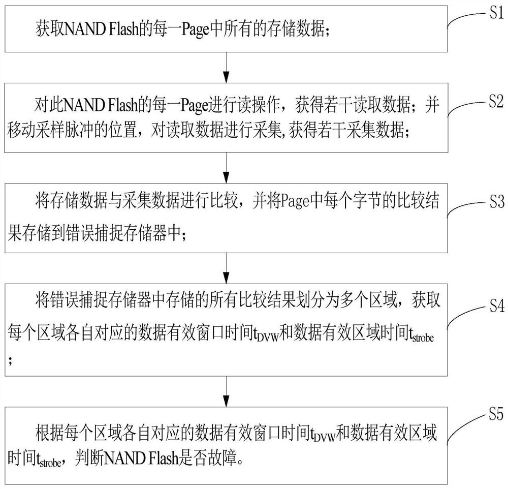
[0043] At present, due to the high degree of chip integration, testing of NAND Flash chips is usually performed by automatic test equipment (ATE); during the test process, it is judged whether the chip has a fault by comparing whether the data input and output by the chip are the same.

[0044] DDR3 mode has more data selection pulse (DQS) than SDR mode. The DQS signal is generated inside the chip after the read operation is enabled, and is used to accurately distinguish each transmission cycle within one c...


PUM


Abstract

The invention discloses a NAND Flash timing test method, the steps comprising: obtaining all stored data in the NAND Flash; performing a read operation on the NAND Flash, and moving the sampling pulse position, collecting the read data, and obtaining a plurality of collected data; The stored data is compared with the collected data, and the comparison result of each byte in the Page is stored in the error capture memory; the error capture memory is divided into multiple areas, and the data valid window time t corresponding to each area is obtained DVW and data valid area time t strobe ;According to the corresponding t of each region DVW and t strobe , to determine whether the NAND Flash is faulty. This timing test method uses a sub-regional method to test the timing parameters to make the measured parameters more accurate. The application of multi-clock setting memory enables ATE to overcome the interference caused by the timing offset of the chip in DDR3 mode and correctly collect the output data of the chip. Functional testing provides a reliable testing environment without improving the hardware of ATE equipment, saving testing costs.

Description

technical field [0001] The invention relates to the technical field of memory chip testing, in particular to a NAND Flash timing testing method. Background technique [0002] At present, due to the high degree of chip integration, testing of NAND Flash chips is usually performed by automatic test equipment (ATE); during the test process, it is judged whether the chip has a fault by comparing whether the data input and output by the chip are the same. [0003] Most of the existing NAND Flash chip interfaces are in DDR3 mode. In DDR3 mode, the data transmission rate is 800MT / S, and the data transmission cycle is 2.5ns. As the data transmission rate increases, the parasitic capacitance interference caused by defects caused by the ATE process The phenomenon will be amplified; specifically, when the operating frequency of the chip is high, the charge stored in the parasitic capacitance will interfere with the circuit characteristics. Because the pulse interval is too short, the ...

Claims


Application Information

Patent Timeline
Patent Type & Authority Patents(China)
IPC IPC(8): G11C29/56G06F11/22
CPCG06F11/2205G06F11/2268G06F11/2273G11C29/56G11C29/56008
Inventor 刘琦韦亚一董立松
Owner INST OF MICROELECTRONICS CHINESE ACAD OF SCI
Why Eureka
Try Eureka