Display device

A display device and display panel technology, which is applied in the direction of optical filters, optics, instruments, etc., can solve the problems that the borderless design cannot be realized, and achieve the effect of ensuring the sense of design

Pending Publication Date: 2020-02-21
BOE TECH GRP CO LTD +1
View PDF4 Cites 12 Cited by
  • Summary
  • Abstract
  • Description
  • Claims
  • Application Information

AI Technical Summary

Problems solved by technology

In the current borderless display device, on the side where the COF Bonding (chip-on-film bonding) area of ​​the display panel is located, the array substrate of the display panel exceeds the color filter substrate to form a step edge. Due to the existence of the COF Bonding structure and the step edge, resulting in Borderless design cannot be realized on the side where the COF Bonding area of ​​the display panel is located

Method used


Image

  • Display device
  • Display device
  • Display device

Examples


Embodiment 1

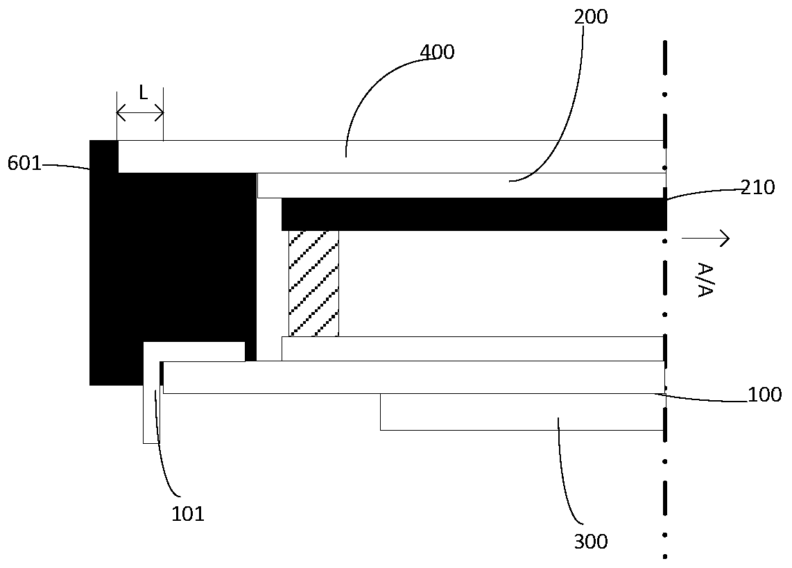
[0063] figure 1 Shown is a schematic structural diagram of the first embodiment of the display device provided by the present invention.

[0064] Such as figure 1 As shown, in this embodiment, the filling part includes: a black filling glue 601 filled between the second polarizer 400 and the binding area of ​​the second substrate 200. A black matrix 210 is provided on the side of the second substrate 200 facing the first substrate 100, and the black filler 601 and the black matrix 210 located at the edge of the second substrate 200 jointly form a light-shielding structure.

[0065] In this structure, the black filler 601 is used to absorb light leakage on the binding side of the display panel. The structure is simple and the implementation process is simple. It only needs to fill black on the binding side after the first substrate 100 and the second substrate 200 are paired. Filling glue 601 is sufficient, which can reduce the complexity of the manufacturing process and reduce the ...

Embodiment 2

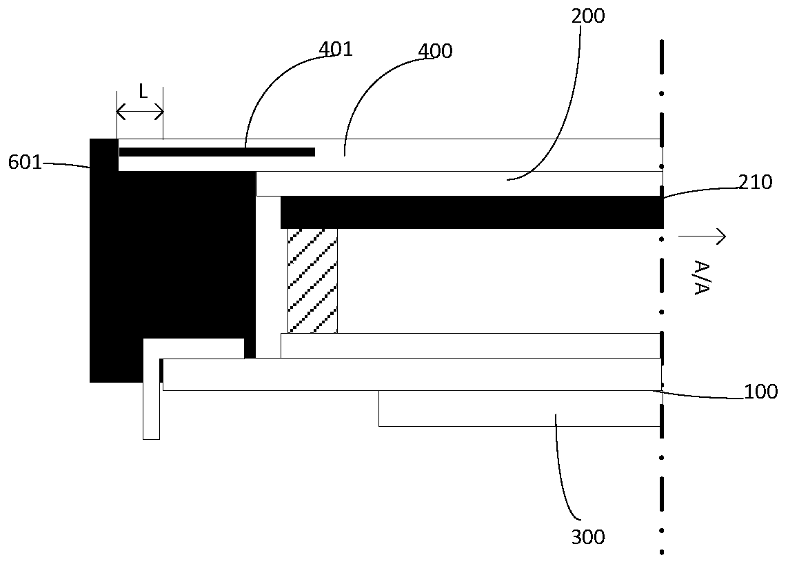
[0073] image 3 Shown is a schematic structural diagram of a second embodiment of the display device provided by the present invention.

[0074] Such as image 3 As shown, the difference between this embodiment 2 and embodiment 1 is that: in the display device provided in this embodiment 2, on the binding side of the display panel, the edge of the second polarizer 400 is further provided with A light-shielding layer 401; in a direction perpendicular to the base substrate of the first substrate, the light-shielding layer 401 covers at least the gap between the black filler 601 and the black matrix 210, and the light-shielding layer 401 The display area of ​​the display panel is not covered.

[0075] With the above solution, in order to further ensure that the gap between the black filler 601 and the black matrix 210 on the second substrate 200 causes light leakage, a light shielding layer 401 may be further provided on the edge of the binding side of the second polarizer 400, The c...

Embodiment 3

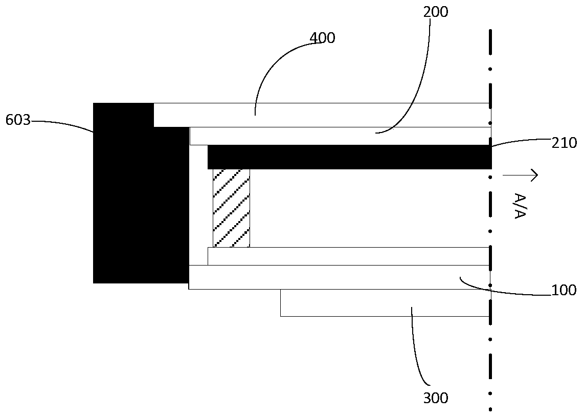
[0080] Figure 4 Shown is a schematic structural diagram of a third embodiment of the display device provided by the present invention.

[0081] Such as Figure 4 As shown, in this embodiment, the filling portion includes: a filling glue 602 filled between the second polarizer 400 and the binding area of ​​the second substrate 200; and The black frame glue 603 outside the filler 602;

[0082] On the binding side of the display panel, the edge of the second polarizer 400 is provided with a light-shielding layer 401. In a direction perpendicular to the base substrate of the first substrate, the light-shielding layer 401 covers at least the The gap between the black frame glue and the black matrix, and the light shielding layer does not cover the display area of ​​the display panel;

[0083] Wherein, the black frame glue 603 overlaps with the projection of the light shielding layer 401 in a direction perpendicular to the base substrate of the first substrate, and the light shielding la...


PUM

PropertyMeasurementUnit
lengthaaaaaaaaaa

Abstract

The invention provides a display device. The display device comprises: a display panel comprising a first substrate and a second substrate which are oppositely arranged, and a binding side, wherein atthe binding side, the substrate of the first substrate exceeds the substrate of the second substrate, and a binding area is formed on the first substrate; a first polaroid arranged on one side, far away from the second substrate, of the first substrate; and a second polaroid arranged on one side, far away from the first substrate, of the second substrate, wherein at the binding side of the display panel, the edge of the second polaroid exceeds the edge of the substrate of the second substrate, a gap is formed between the part, exceeding the edge of the substrate of the second substrate, of the edge of the second polaroid and the binding area on the first substrate, and a filling part is arranged in the gap. According to the invention, the display device can achieve a four-side frameless design.

Description

Technical field [0001] The present invention relates to the field of display technology, and in particular to a display device. Background technique [0002] With the continuous development of the display industry, borderless display technology has become a mainstream direction for the development of the display field. In the current borderless display device, the COF Bonding area of ​​the display panel is located on the side of the display panel, and the array substrate of the display panel extends beyond the color filter substrate to form stepped edges. Due to the COF bonding structure and the stepped edges, The borderless design cannot be realized on the side of the COF Bonding area of ​​the display panel. Summary of the invention [0003] The purpose of the present invention is to provide a display device that can realize a four-sided borderless design and prevent light leakage. [0004] The technical solutions provided by the present invention are as follows: [0005] A displa...

Claims


Application Information

Patent Timeline
Patent Type & Authority Applications(China)
IPC IPC(8): G02F1/1333G02F1/1335G02F1/1339
CPCG02F1/1333G02F1/133528G02F1/133512G02F1/1339G02B5/003G02B5/201G02B5/3025G06F1/1637G02F1/13332G02F1/133314G02F2202/28G06F1/1601G06F2200/1612G02B5/20
Inventor 陈轶夫薄灵丹曲莹莹董霆吕志宇黄建华
Owner BOE TECH GRP CO LTD
Why Eureka
Try Eureka