Substrate and liquid crystal display panel

A substrate and overlapping area technology, applied in nonlinear optics, instruments, optics, etc., can solve the problems of high power consumption of display panels and low aperture ratio of display panels, reduce the degree and width of light leakage, and improve transmittance , the effect of reducing the electric field strength

Inactive Publication Date: 2020-02-21
SHENZHEN CHINA STAR OPTOELECTRONICS SEMICON DISPLAY TECH CO LTD
View PDF10 Cites 15 Cited by
  • Summary
  • Abstract
  • Description
  • Claims
  • Application Information

AI Technical Summary

Problems solved by technology

[0005] Embodiments of the present invention provide a substrate and a liquid crystal display panel, which are used to solve the problem of the display panel in the prior art. Due to the large overlapping area between the black matrix and the pixel electrodes, the aperture ratio of the display panel is low, resulting in the power of the display panel. expensive technical issues

Method used


Image

  • Substrate and liquid crystal display panel
  • Substrate and liquid crystal display panel
  • Substrate and liquid crystal display panel

Examples


Embodiment Construction

[0026] The following will clearly and completely describe the technical solutions in the embodiments of the present invention with reference to the accompanying drawings in the embodiments of the present invention. Obviously, the described embodiments are only some, not all, embodiments of the present invention. Based on the embodiments of the present invention, all other embodiments obtained by those skilled in the art without making creative efforts belong to the protection scope of the present invention.

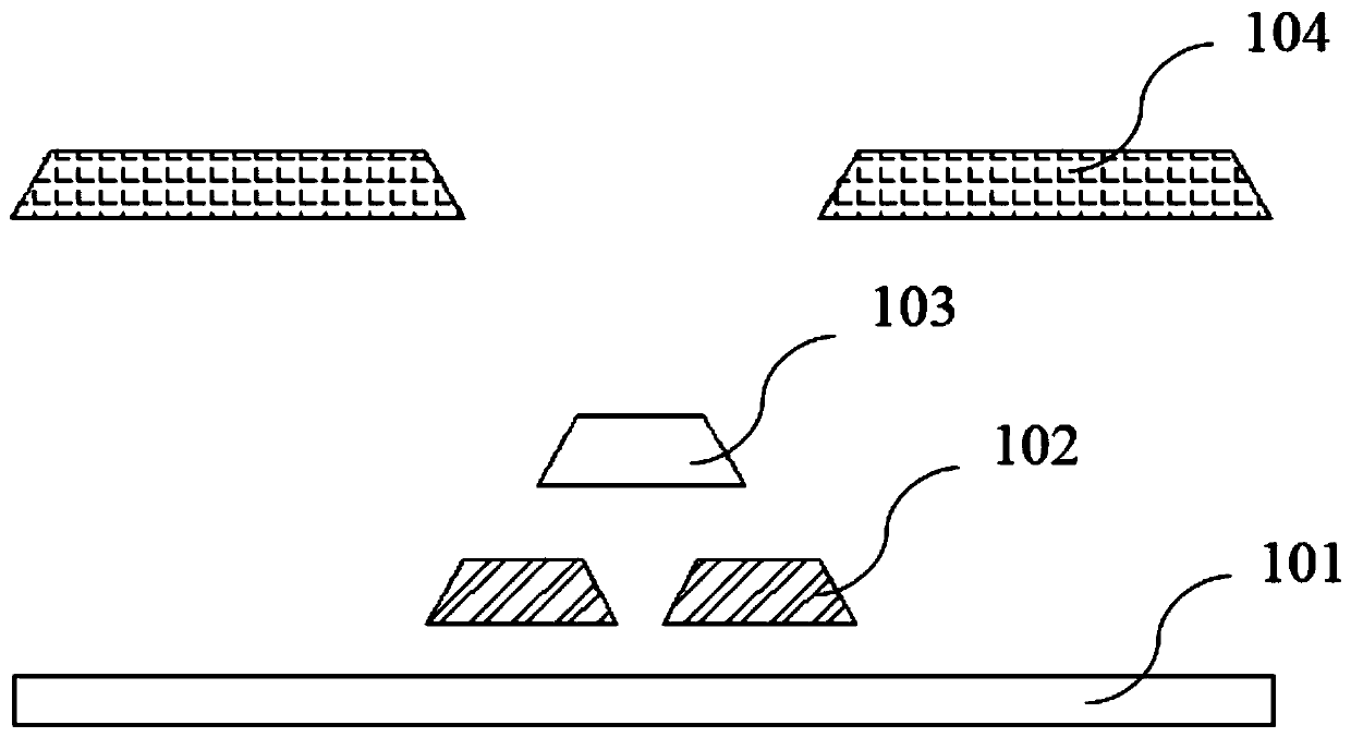
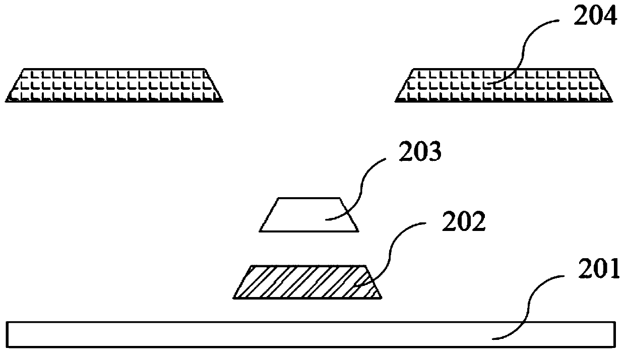
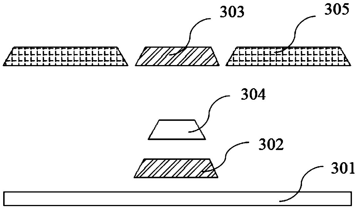
[0027] Such as figure 1 As shown, the basic structural diagram of the substrate provided by Embodiment 1 of the present invention, from which the various components of the present invention and the relative positional relationship between the various components can be seen intuitively. The substrate includes a substrate 101 , a light-shielding metal layer, a signal line layer, and a pixel electrode layer; the light-shielding metal layer is located on the substrate 101, an...


PUM


Abstract

The invention provides a substrate. The substrate comprises a substrate body, a shading metal layer, a signal line layer and a pixel electrode layer. The shading metal layer is located on the substrate and is patterned to form a shielding electrode; the signal line layer is patterned to form a data line; the pixel electrode layer is patterned to form a pixel electrode; and the orthographic projection of the data line on the substrate and the orthographic projection of the shielding electrode on the substrate have an overlapping area. According to the invention, the overlapping area of the shielding electrode and the data line is increased; therefore, the shielding electrode shields the electric field of the data line more, the electric field intensity between the data line and the pixel electrode is reduced, the degree and width of light leakage are both reduced, namely, the width of the light leakage are shielded by a black matrix is reduced, the overlapping area between the black matrix and the pixel electrode is reduced, the aperture ratio f the display panel is improved, the penetration rate of the display panel is increased, and the power consumption of the display panel is reduced.

Description

technical field [0001] The invention relates to the field of display technology, in particular to a substrate and a liquid crystal display panel. Background technique [0002] Thin Film Transistor-Liquid Crystal Display (TFT-LCD) is widely used in mobile phones, tablet computers, TVs and other products. Generally speaking, a liquid crystal display panel is a liquid crystal layer sandwiched between two parallel upper and lower substrates. between them, and apply a voltage to the electrodes of the upper and lower substrates to generate an electric field between the two substrates to control the tilting direction of the liquid crystal molecules in the liquid crystal layer, thereby displaying different pictures. With the increasing acceptance of liquid crystal display devices in the market With the increase, consumers have higher and higher requirements on the quality of liquid crystal display devices, such as viewing angle, contrast ratio, picture response rate, power consumpti...

Claims


Application Information

Patent Timeline
Patent Type & Authority Applications(China)
IPC IPC(8): G02F1/1362
CPCG02F1/136209G02F1/136286G02F1/136218G02F1/136222G02F1/134309
Inventor 肖偏
Owner SHENZHEN CHINA STAR OPTOELECTRONICS SEMICON DISPLAY TECH CO LTD
Why Eureka
Try Eureka