Method for manufacturing non-volatile memory cell

Active Publication Date: 2005-03-22
POWERCHIP SEMICON MFG CORP
View PDF2 Cites 4 Cited by
  • Summary
  • Abstract
  • Description
  • Claims
  • Application Information

AI Technical Summary

Benefits of technology

Accordingly, one object of the present invention is to provide an improved non-volatile memory cell structure having reduced numbers of polysilicon layer and increased overlapping area between control gate and floating gates.
It is advantageous to use the present invention because the control gate of the non-volatile memory cell is located between two floating gates, thereby increasing the overlapping area between the control gate and the floating gates. The overlapping area includes the sidewalls of the floating gates and a portion of the top surface of the floating gates. This results in an increased coupling ratio. Furthermore, the split gates and the control gate are formed by etching the same polysilicon layer (second polysilicon layer). Only two layers of polysilicon are needed to complete the non-volatile memory cell of this invention. By doing this, the manufacturing process for the novel non-volatile memory cell structure of this invention can be well compatible with the manufacturing process for the peripheral circuit.

Problems solved by technology

However, the above-mentioned prior art non-volatile memory cell structure is quite not compatible with the manufacturing process for the peripheral logic circuit.
Moreover, the coupling ratio of the above-mentioned prior art non-volatile memory cell structure is still low.

Method used


Image

  • Method for manufacturing non-volatile memory cell
  • Method for manufacturing non-volatile memory cell
  • Method for manufacturing non-volatile memory cell

Examples


Embodiment Construction

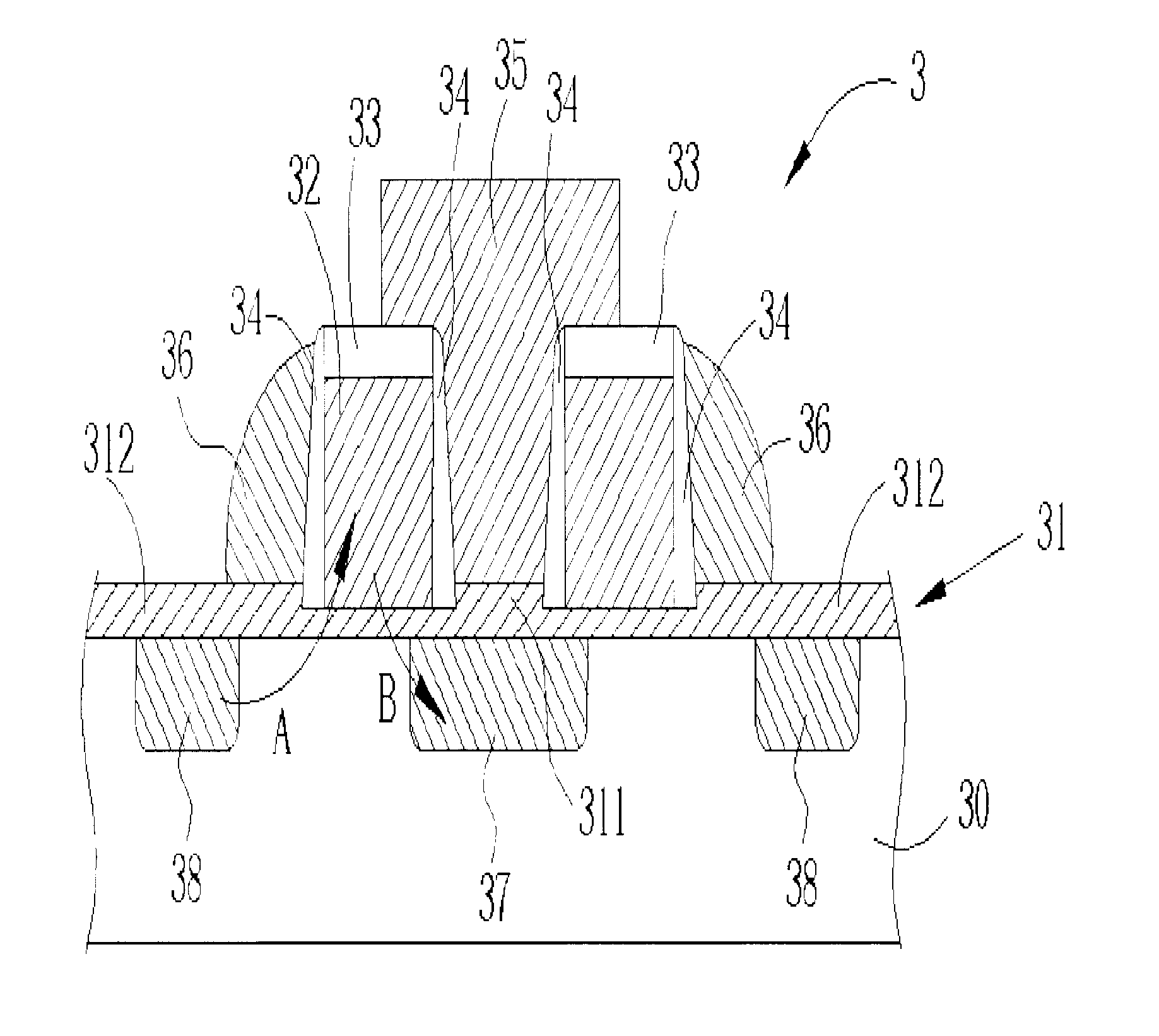
The preferred embodiment in accordance with the present invention will be discussed in detail with reference to FIG. 3, in which like reference numerals designate similar or corresponding elements, regions, and portions. It is understood that the type of semiconductor regions and device layout are chosen solely for illustration, and persons having ordinary skill in the art would recognize other alternatives, variations, and modifications.

Please refer to FIG. 3. FIG. 3 is a cross-sectional, schematic diagram illustrating a non-volatile memory cell structure 3 according to the preferred embodiment of the present invention. The non-volatile memory cell structure 3 includes a substrate 30, a tunneling oxide layer 31, floating gates 32, a dielectric layer 33, a plurality of spacers 34, a control gate 35, and split gates 36.

In this embodiment, the substrate 30 is a P type silicon substrate. Three spaced-apart doped regions are provided in the substrate 30. Dopants such as elements of the ...


PUM


Abstract

A non-volatile memory cell having a symmetric cell structure is disclosed. The non-volatile memory cell includes a substrate, a tunnel oxide layer, two floating gates, a dielectric layer, a plurality of spacers, a control gate, and two split gates. The substrate has at least two sources and a drain that is located between the sources. The floating gates are formed on the tunneling oxide layer, and each of floating gates is located between each source and the drain. The dielectric layer is formed on the floating gates. The control gate is formed over the drain and is between the floating gates. The split gates are located adjacent to outward sidewalls of the floating gates, respectively. Therefore, each of the split gates is opposite to the control gate through each of the floating gates.

Description

BACKGROUND OF INVENTION1. Field of the InventionThe present invention relates to memory fabrication. More specifically, the present invention relates to a method for manufacturing non-volatile memory cells.2. Description of the Prior ArtComputer storage media technology is evolving rapidly. While hard drives and CD-ROMs will still be around for years to come because of their high capacity and low cost, new forms of storage are constantly being developed. One technology that appears to have distinct advantages over conventional forms of storage is flash memory. Like conventional storage systems, flash memory is nonvolatile, requiring no power to maintain the stored information, and rewriteable.FIG. 1 is a sectional schematic diagram illustrating a prior art non-volatile memory cell structure1. As shown in FIG. 1, prior art non-volatile memory cell structure1 includes a substrate 10, a tunneling oxide layer 11 formed on the substrate 10, a floating gate 12 formed on the tunneling oxid...

Claims


Application Information

Patent Timeline
IPC IPC(8): H01L21/70H01L27/115H01L29/423H01L29/66H01L29/40H01L21/8247H01L29/788
CPCH01L27/115H01L29/7883H01L29/42324H01L27/11521H10B69/00H10B41/30
Inventor CHANG, KO-HSINGHSU, CHENG-YUAN
Owner POWERCHIP SEMICON MFG CORP
Why Eureka
Try Eureka