Non-volatile memory and fabricating method thereof

a non-volatile memory and fabricating method technology, applied in the field of semiconductor devices, can solve the problems of increasing device integration and inability to increase gcr, and achieve the effects of enhancing gcr, improving device performance, and increasing overlapped area

Active Publication Date: 2012-06-28
POWERCHIP SEMICON MFG CORP
View PDF9 Cites 3 Cited by
  • Summary
  • Abstract
  • Description
  • Claims
  • Application Information

AI Technical Summary

Benefits of technology

[0008]Accordingly, the invention provides a non-volatile memory and a fabricating method thereof, so as to increase the overlapped area between the floating gate and the control gate, to enhance the GCR, to improve device performance, and to significantly reduce the interference between the floating gates.
[0016]In addition, the protruding portion of the floating gate is fully covered and surrounded by the control gate in any direction, such as an extending direction of a bit line, an extending direction of a word line and an extending direction of an included angle formed between a word line and a bit line. Therefore, the overlapped area between the floating gate and the control gate is increased to enhance the GCR of the memory. Generally, the higher the gate coupling ratio is, the lower operation voltage of the memory needs, thereby increasing the efficiency of the device. Furthermore, the protruding portion of the floating gate is surrounded by the control gate, so as to reduce the interference between the adjacent floating gates.
[0026]In the fabricating method of a non-volatile memory of the invention, the floating gate having the protruding portion is formed. The protruding portion of the floating gate is fully covered and surrounded by the control gate in any direction, such as an extending direction of a bit line, an extending direction of a word line and an extending direction of an included angle formed between a word line and a bit line. In other words, the protruding portion of the floating gate is covered and surrounded by the control gate in all directions. Therefore, the overlapped area between the floating gate and the control gate is increased to enhance the GCR of the memory. Accordingly, the lower operation voltage of the memory is required as the gate coupling ratio is increased, and thus the efficiency of the device is increased.
[0027]In the fabricating method of a non-volatile memory of the invention, the mask used to form the conductive layer having the protruding portions adapts the same mask for the subsequent formed control gates (word lines), so that additional masks are not required and the manufacturing cost is reduced.

Problems solved by technology

However, as the integration of the device becomes higher, it is difficult to increase the overlapped area between the control gate and the floating gate in the conventional stacked gate structure, and it therefore has the issues for incapable of increasing the GCR and increasing the device integration.

Method used


Image

  • Non-volatile memory and fabricating method thereof
  • Non-volatile memory and fabricating method thereof
  • Non-volatile memory and fabricating method thereof

Examples


Embodiment Construction

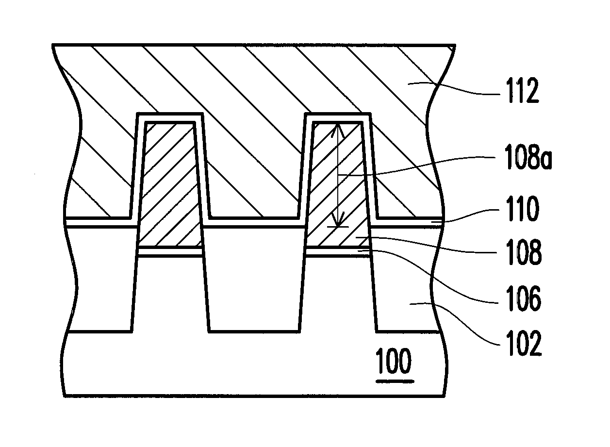
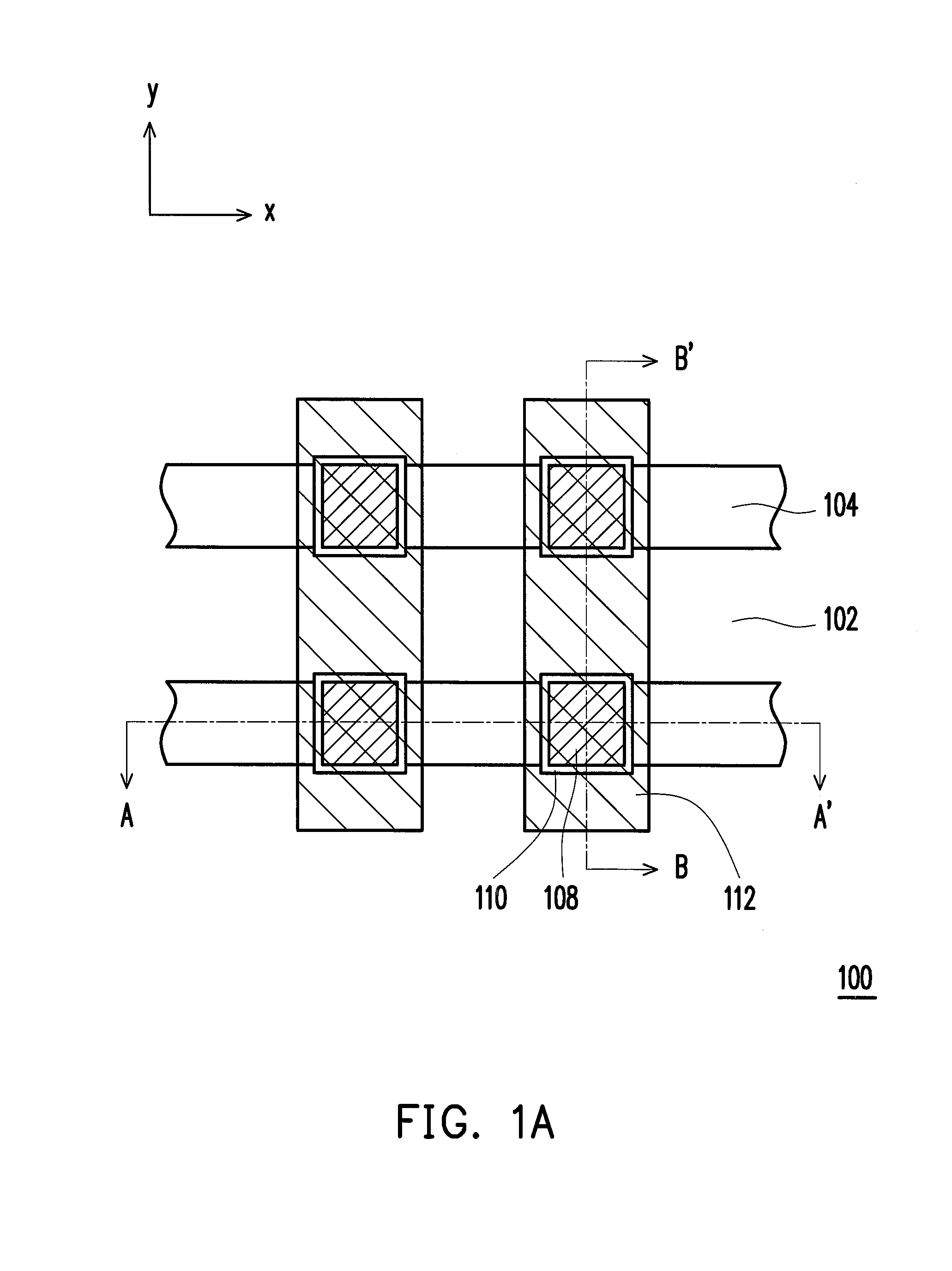
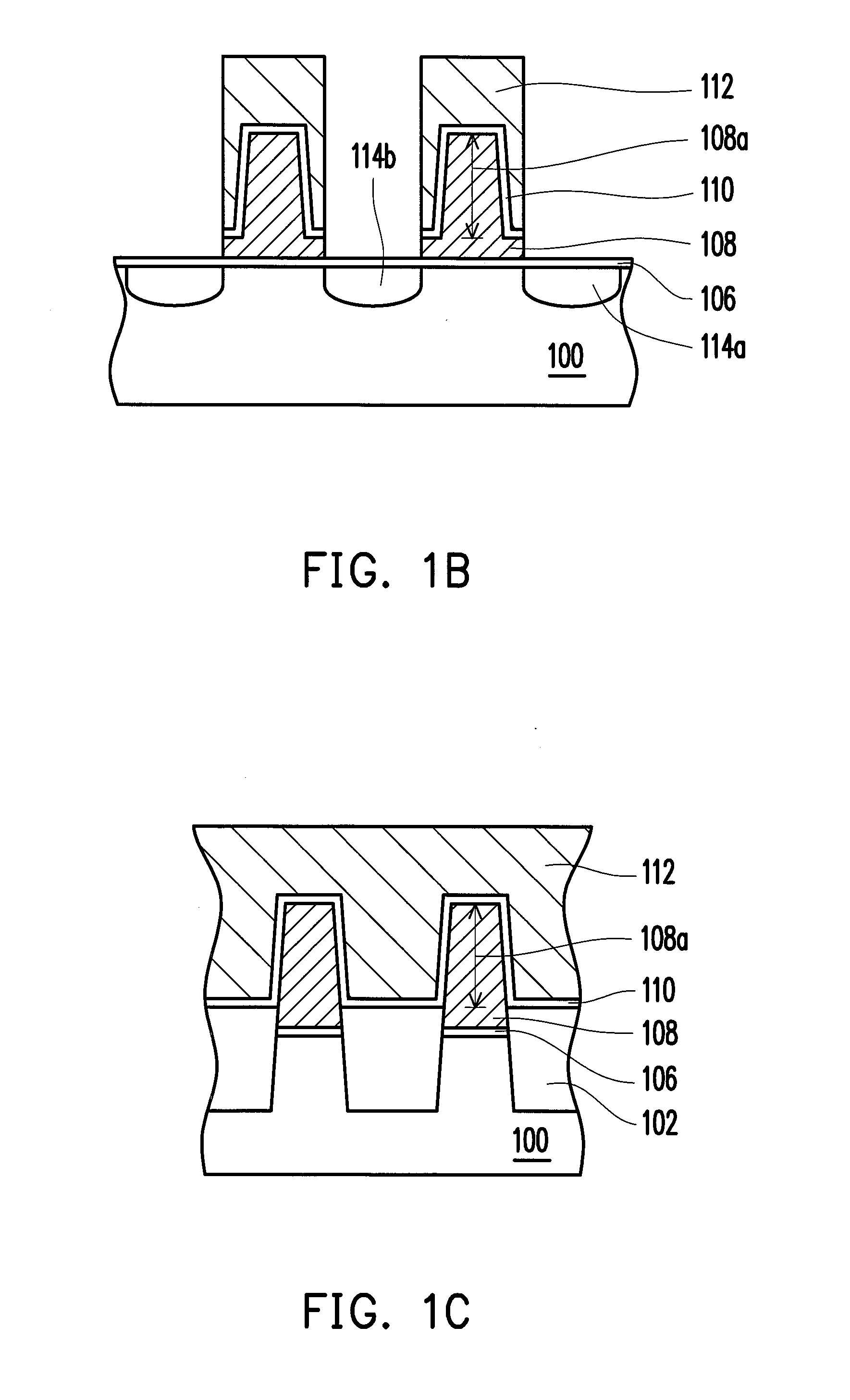
[0035]FIG. 1A shows a top view of a non-volatile memory according to an embodiment of the invention. FIG. 1B is a cross-sectional view taken along a line A-A′ depicted in FIG. 1A. FIG. 1C is a cross-sectional view taken along a line B-B′ depicted in FIG. 1A. The line A-A′ is a cutting line along the active region, and the line B-B′ is a cutting line along the word line.

[0036]Referring to FIGS. 1A to 1C, the non-volatile memory is disposed on a substrate 100, for example. The non-volatile memory includes isolation structures 102, control gates (word lines) 112, floating gates 108, a tunneling dielectric layer 106, an inter-gate dielectric layer 110 and a plurality of doping regions 114a, 114b.

[0037]The isolation structures 102 are disposed in parallel in the substrate 100 to define an active regions 104, for example. The isolation structures 102 can extend in an X direction. The isolation structures 102 can be shallow trench isolation structures.

[0038]The control gates (word lines) ...


PUM


Abstract

A non-volatile memory having a tunneling dielectric layer, a floating gate, a control gate, an inter-gate dielectric layer and a first doping region and a second doping region is provided. The tunneling dielectric layer is disposed on a substrate. The floating gate is disposed on the tunneling dielectric layer, and has a protruding portion. The control gate is disposed over the floating gate to cover and surround the protruding portion. The protruding portion of the floating gate is fully covered and surrounded by the control gate in any direction, including extending directions of bit lines, word lines and an included angle formed between the word line and the bit line. The inter-gate dielectric layer is disposed between the floating gate and the control gate. The first doping region and the second doping region are respectively disposed in the substrate at two sides of the control gate.

Description

CROSS-REFERENCE TO RELATED APPLICATION[0001]This application claims the priority benefit of Taiwan application serial no. 99145267, filed on Dec. 22, 2010. The entirety of the above-mentioned patent application is hereby incorporated by reference herein and made a part of this specification.BACKGROUND OF THE INVENTION[0002]1. Field of the Invention[0003]The invention relates to a semiconductor device and a fabricating method thereof. More particularly, the invention relates to a non-volatile memory and a fabricating method thereof.[0004]2. Description of Related Art[0005]Non-volatile memory is a kind of memory having the advantages that it allows multiple data storing, reading or erasing operations. The data stored in the non-volatile memory will be retained even if the power applied to the device is cut off. The non-volatile memory has become a widely adopted memory device in personal computers and electronic equipments.[0006]A typical non-volatile memory device is a stacked gate s...

Claims


Application Information

Patent Timeline
Patent Type & Authority Applications(United States)
IPC IPC(8): H01L29/788H01L21/28
CPCH01L27/11521H01L29/66825H01L21/76224H01L29/7881H10B41/30
Inventor LEE, YA-JUILIN, YING-CHIA
Owner POWERCHIP SEMICON MFG CORP
Why Eureka
Try Eureka