TFT array substrate and OLED panel

An array substrate and panel technology, applied in the direction of electrical components, electric solid devices, circuits, etc., can solve the problem that the lower frame of the OLED panel cannot be further reduced, and achieve the effect of preventing bending and breaking and reducing the length

Inactive Publication Date: 2020-02-28
WUHAN CHINA STAR OPTOELECTRONICS SEMICON DISPLAY TECH CO LTD
View PDF4 Cites 2 Cited by
  • Summary
  • Abstract
  • Description
  • Claims
  • Application Information

AI Technical Summary

Problems solved by technology

However, in this way, in order to prevent various traces from contacting each other, the wire change position 33 needs to avoid the design positions of the VDD trace 4 and the VSS trace area 5, so that the lower frame of the OLED panel cannot be further reduced

Method used


Image

  • TFT array substrate and OLED panel
  • TFT array substrate and OLED panel
  • TFT array substrate and OLED panel

Examples


Embodiment Construction

[0026] The following descriptions of the various embodiments refer to the accompanying drawings to illustrate specific embodiments in which the present invention can be practiced. Furthermore, the directional terms mentioned in the present invention are, for example, up, down, top, bottom, front, back, left, right, inside, outside, side, surrounding, central, horizontal, transverse, vertical, longitudinal, axial, The radial direction, the uppermost layer or the lowermost layer, etc. are only directions referring to the attached drawings. Therefore, the directional terms used are used to illustrate and understand the present invention, but not to limit the present invention.

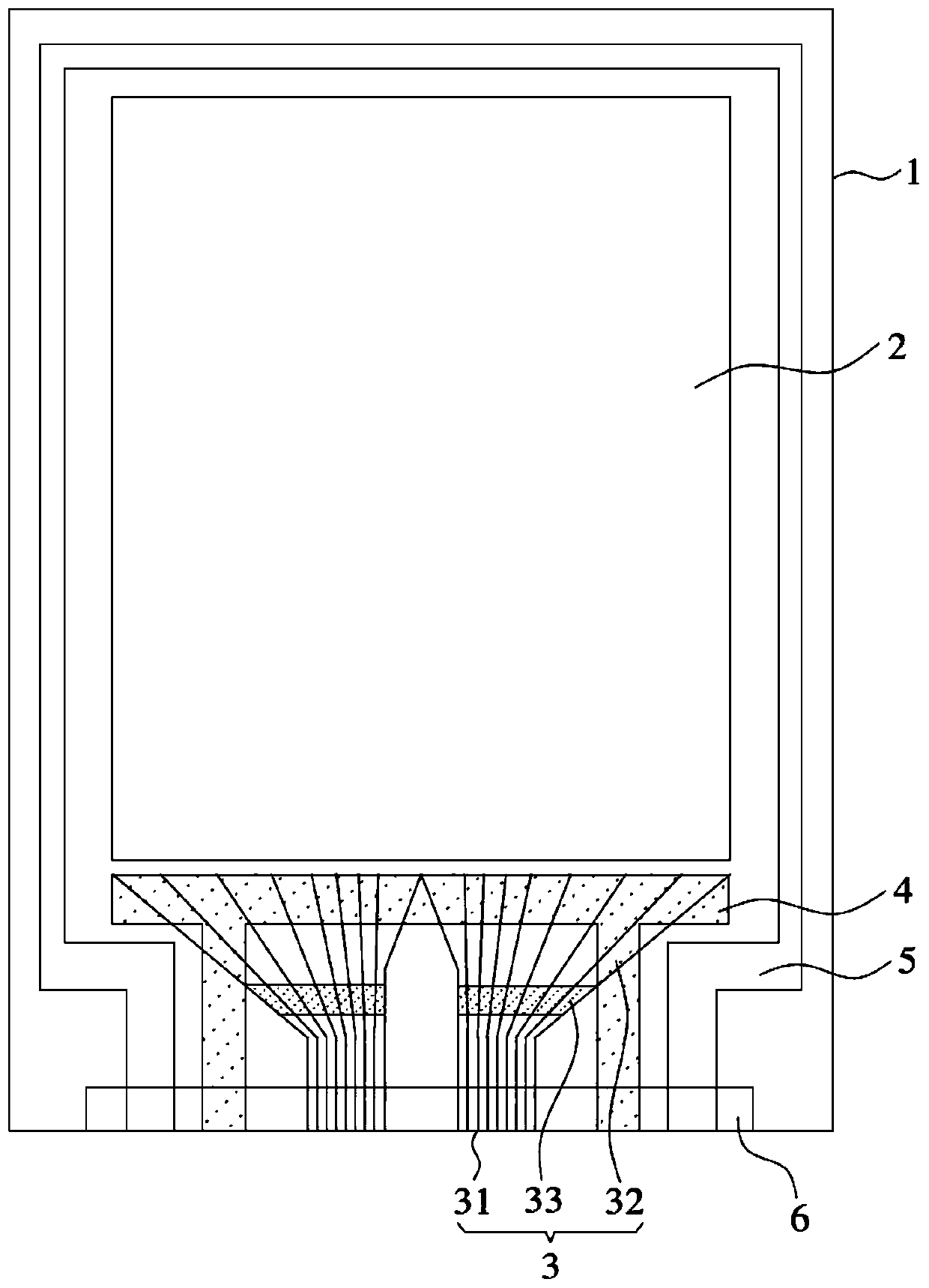
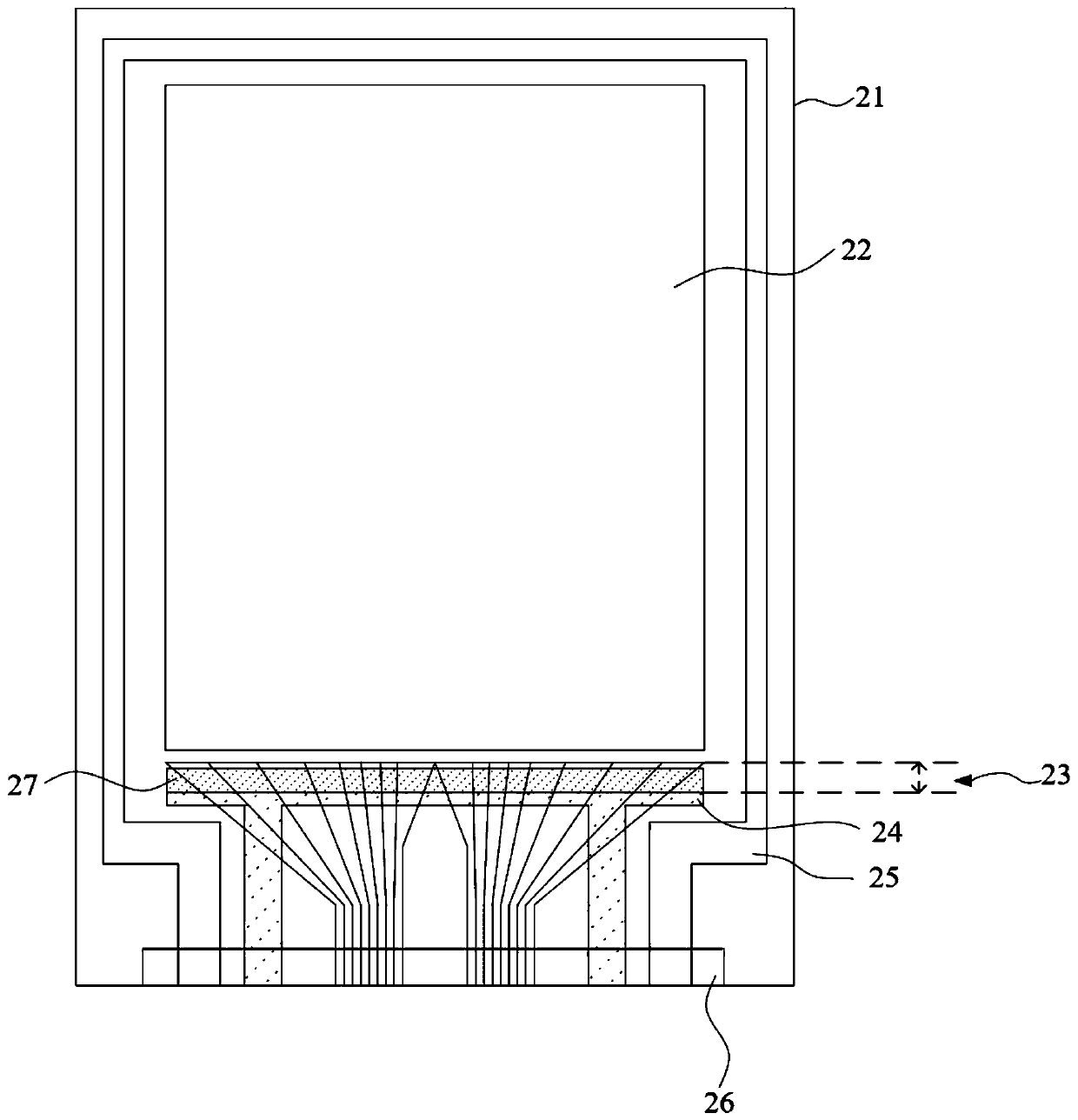
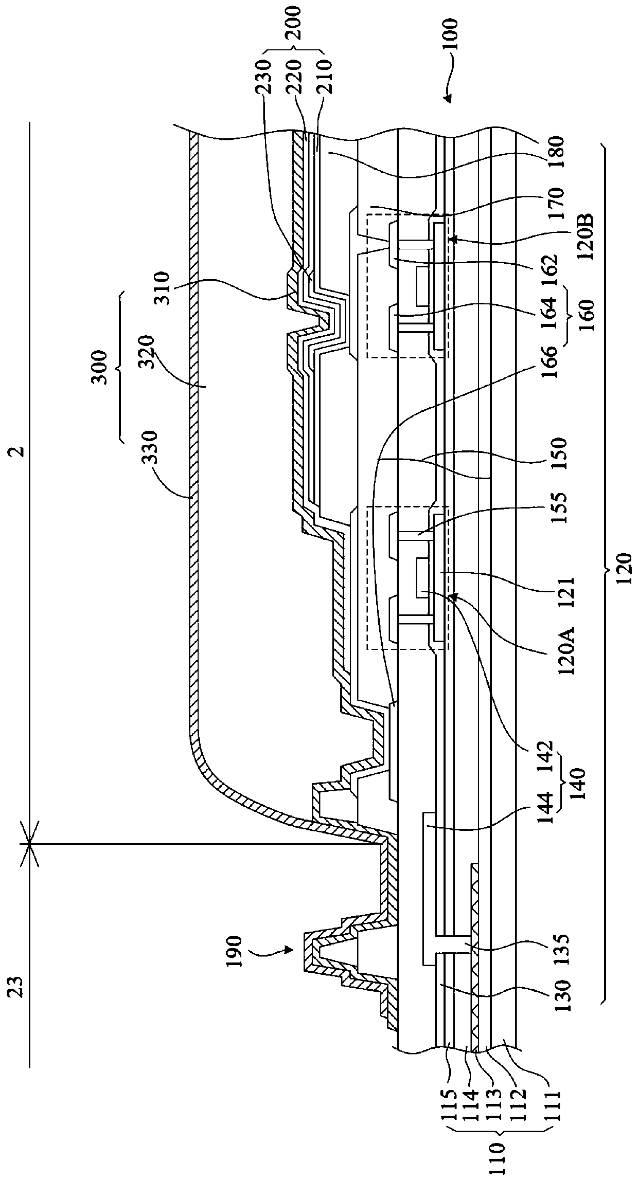
[0027] Please refer to figure 2 and image 3 , figure 2 It is a schematic diagram of circuit configuration of an OLED panel according to an embodiment of the present invention, image 3 yes figure 2 Structural sectional view of embodiment. The OLED panel of this embodiment includes: a TFT array s...


PUM


Abstract

The invention discloses a TFT array substrate and an OLED panel. The TFT array substrate includes a display area and a non-display area. The non-display area is provided with a gate line connected toa control chip. The TFT array substrate includes a flexible substrate. The flexible substrate includes a metal line change sublayer in the non-display area and close to the display area; and a thin film transistor layer disposed on the flexible substrate and including a plurality of thin film transistors corresponding to the display area, wherein the gate line of each of the thin film transistor layers and the gate line of the non-display area are changed through the metal line change sublayer.

Description

technical field [0001] The invention relates to the field of display technology, in particular to a TFT array substrate and an OLED panel. Background technique [0002] Organic light emitting diode (OLED) has many excellent characteristics such as self-illumination, low energy consumption, wide viewing angle, rich colors, fast response, and flexible screens can be prepared. The related design has become a development trend in the field of display technology. Among them, reducing the width of the non-display area at the edge of the OLED panel is one of the main issues. [0003] In the current common OLED panel design, such as figure 1 As shown, the scanning lines, data lines and grounding lines of the TFT array in the display area 2 are respectively connected to the Chip on film area (chip on film, COF). Since the gate wiring is located on the gate metal layer, and the VDD wiring 4 and the VSS wiring 5 are located in the source-drain layer, therefore, the gate wiring 3 wil...

Claims


Application Information

Patent Timeline
Patent Type & Authority Applications(China)
IPC IPC(8): H01L27/12H01L27/32
CPCH01L27/124H10K59/131
Inventor 徐彬许红玉
Owner WUHAN CHINA STAR OPTOELECTRONICS SEMICON DISPLAY TECH CO LTD
Why Eureka
Try Eureka