Low power negative voltage level shifter
A level shifter and negative voltage technology, applied in the direction of reducing power consumption, power reduction of field effect transistors, electrical components, etc., can solve the problems of consuming circuit area and increasing power consumption
- Summary
- Abstract
- Description
- Claims
- Application Information
AI Technical Summary
Problems solved by technology
Method used
Image

Examples
Embodiment Construction
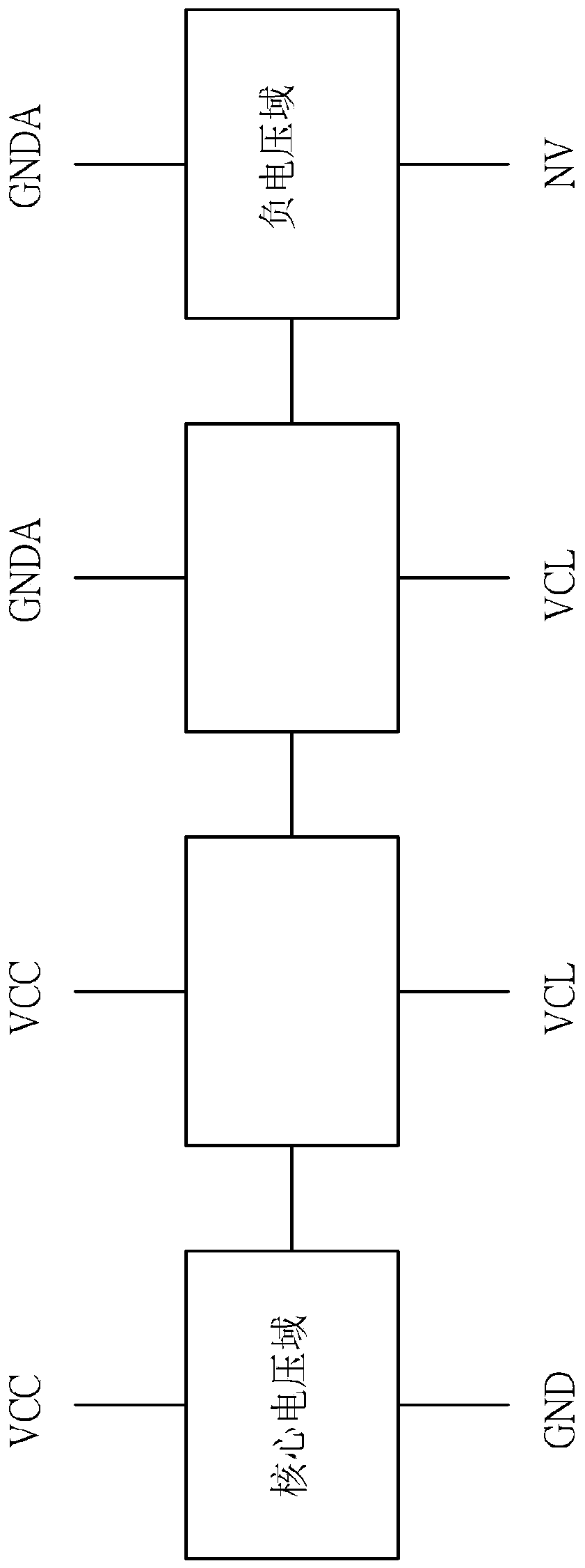
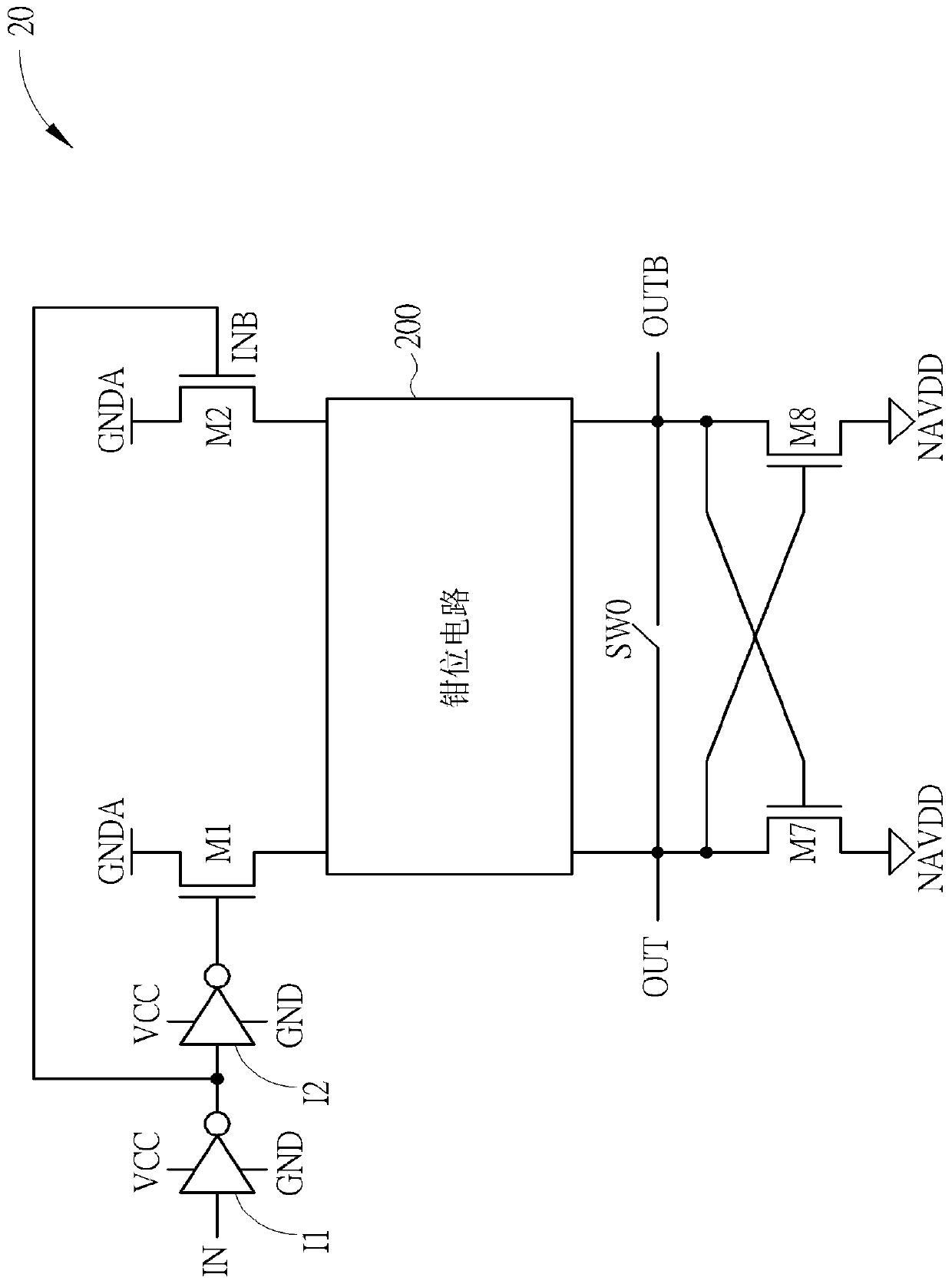
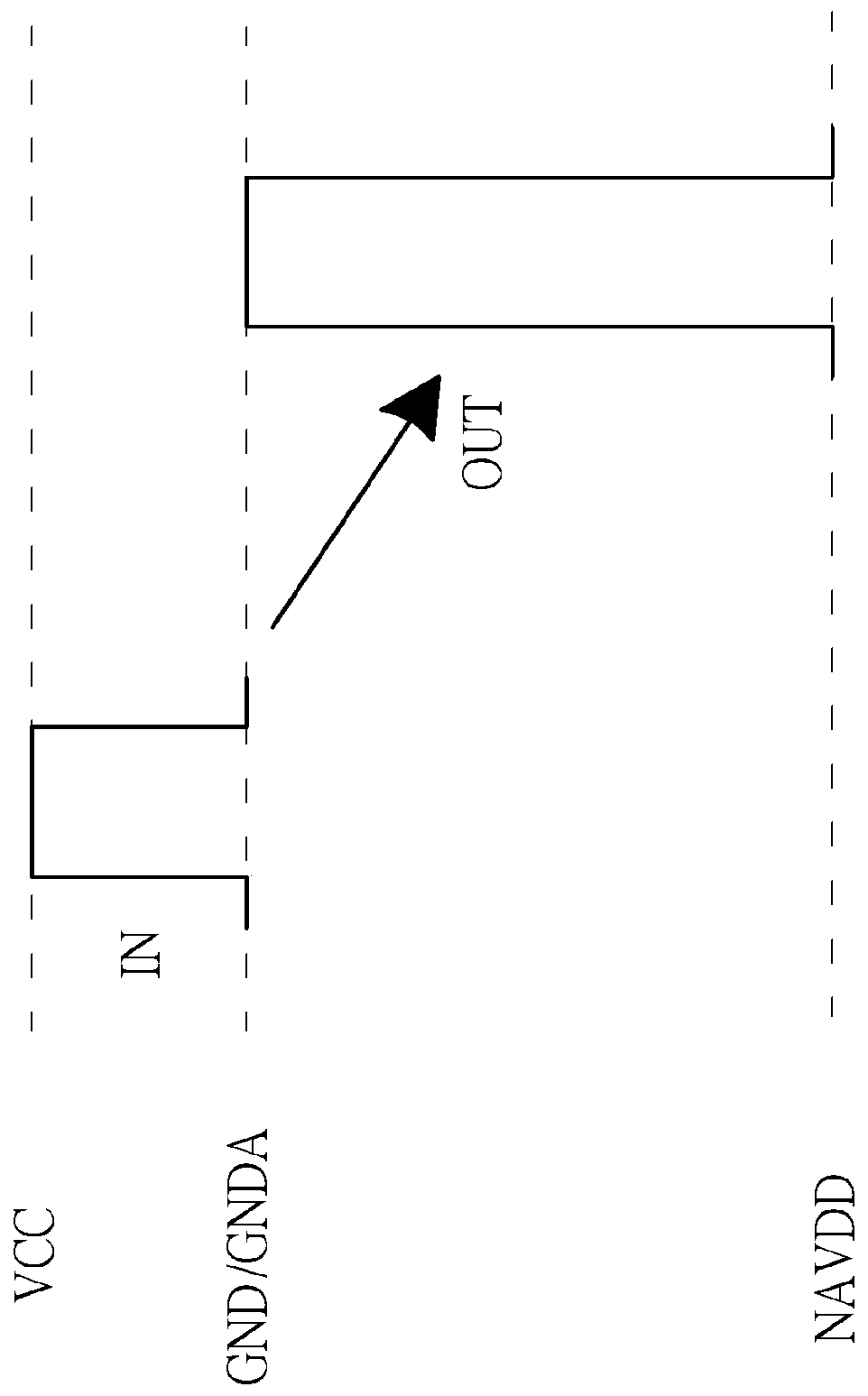
[0043] Please refer to figure 2 , figure 2 It is a schematic diagram of a negative voltage level shifter 20 according to an embodiment of the present invention. Such as figure 2 As shown, the negative voltage level shifter 20 includes an input transistor pair M1 and M2, a clamping circuit 200, an output transistor pair M7 and M8, and a switch SW0. figure 2 Also shown are two inverters I1 and I2 , which may be included in the negative voltage level shifter 20 or provided independently of the negative voltage level shifter 20 . The negative voltage level shifter 20 can receive an input signal IN, and correspondingly output an output signal OUT and an inverted output signal OUTB. More specifically, the inverters I1 and I2 operate within a positive voltage domain VCC˜GND, and the negative voltage level shifter 20 can convert the positive voltage domain VCC˜GND into a negative voltage domain GNDA˜NAVDD. In one embodiment, the voltage VCC may be 1.5V, which is a core voltage...
PUM
 Abstract
Description
Claims
Application Information
 - R&D
- Intellectual Property
- Life Sciences
- Materials
- Tech Scout
- Unparalleled Data Quality
- Higher Quality Content
- 60% Fewer Hallucinations
Browse by: Latest US Patents, China's latest patents, Technical Efficacy Thesaurus, Application Domain, Technology Topic, Popular Technical Reports.
© 2025 PatSnap. All rights reserved.Legal|Privacy policy|Modern Slavery Act Transparency Statement|Sitemap|About US| Contact US: help@patsnap.com