Microled display panel

A technology of micro-light-emitting diodes and display panels, which is applied in the direction of electrical components, electric solid-state devices, circuits, etc., and can solve the problems of large output load of the driver, failure of the display panel to be driven normally, and inability to apply the micro-light-emitting diode display panel, etc.

Inactive Publication Date: 2020-03-17
PRILIT OPTRONICS INC
View PDF7 Cites 3 Cited by
  • Summary
  • Abstract
  • Description
  • Claims
  • Application Information

AI Technical Summary

Problems solved by technology

However, when the size of the display panel becomes larger or the resolution becomes higher, the output load of the driver is too large, and the long delay time makes the display panel unable to drive normally.
Therefore, the passive driving mechanism cannot be applied to large-sized micro-LED display panels

Method used


Image

  • Microled display panel
  • Microled display panel
  • Microled display panel

Examples


Embodiment Construction

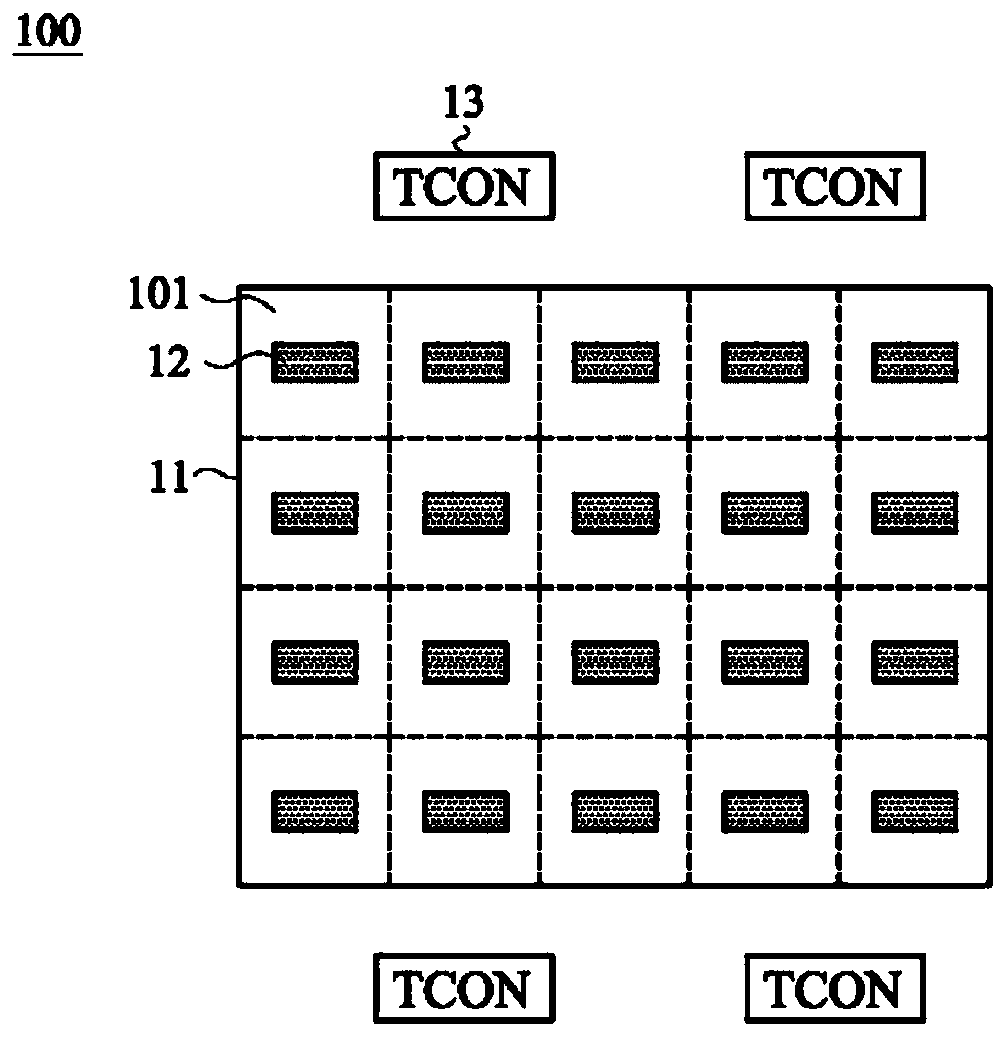
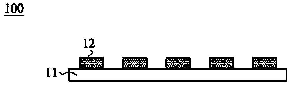
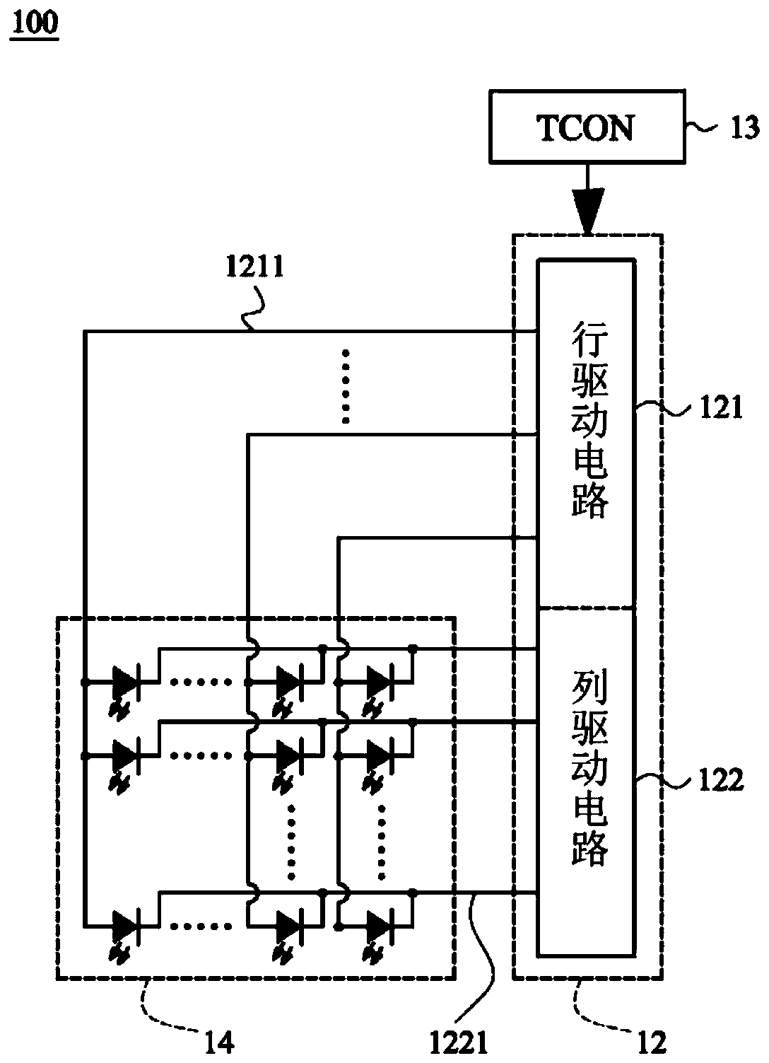
[0080] Figure 1A A top view showing a micro light emitting diode (microLED) display panel 100 according to an embodiment of the present invention, Figure 1B show Figure 1A A side view of the micro light emitting diode display panel 100 . The structure of the micro-LED display panel 100 of this embodiment is preferably suitable for a large-size high-resolution display panel, such as a display panel with a resolution of 3840RGBx2160. In this specification, the size class of the micro light-emitting diodes is 1-10 microns. However, it will be smaller due to the application field of the product or the development of future technology. In this specification, a "large-size" display panel is defined as a display panel larger than 10 inches according to current industry practice. However, the definition of a "large-size" display panel may change due to product application fields or future technological developments. In this specification, a "high-resolution" display panel is def...


PUM


Abstract

A micro light-emitting diode (microLED) display panel includes a plurality of microLEDs; a substrate for supporting the microLEDs, the substrate being divided into a plurality of sub-regions; and a plurality of chip-on-film (COF) packages mounted on surfaces of the sub-regions respectively, a plurality of drivers being disposed on the COF packages respectively. Through the technical scheme, the load of the drivers can be effectively reduced to achieve the single large-size high-resolution microLED display panel.

Description

technical field [0001] The present invention relates to a display panel, in particular to a micro LED display panel. Background technique [0002] A micro LED (microLED, mLED or μLED) display panel is a type of flat panel display, which is composed of individual microscopic light emitting diodes with a size of 1-10 microns. Compared with traditional liquid crystal display panels, micro-light-emitting diode display panels have greater contrast and faster response time, and consume less power. Although micro-light-emitting diodes and organic light-emitting diodes (OLEDs) also have the characteristics of low power consumption, micro-light-emitting diodes have higher Brightness, higher luminous efficacy and longer lifespan. [0003] Active driving using thin film transistors (TFTs) is a commonly used driving mechanism, which can be combined with micro-LEDs to manufacture display panels. However, thin-film transistors use a complementary metal-oxide-semiconductor (CMOS) manufa...

Claims


Application Information

Patent Timeline
Patent Type & Authority Applications(China)
IPC IPC(8): H01L27/15H01L33/48H01L33/62
CPCH01L27/15H01L33/48H01L33/62
Inventor 吴炳昇陈发明
Owner PRILIT OPTRONICS INC
Why Eureka
Try Eureka