Embedded gate structure and manufacturing method thereof

A technology of gate structure and manufacturing method, applied in the field of buried gate structure and its manufacturing, can solve the problem that transistors cannot take into account performance and integration at the same time, so as to improve short-channel effect, improve device integration, and increase device integration. The effect of large drive current

Pending Publication Date: 2020-03-24
CHANGXIN MEMORY TECH INC
View PDF0 Cites 2 Cited by
  • Summary
  • Abstract
  • Description
  • Claims
  • Application Information

AI Technical Summary

Problems solved by technology

[0005] In view of the above-mentioned shortcomings of the prior art, the purpose of the present invention is to provide a buried gate structure and its manufacturing method, which is used to solve the problem that the existing transistors cannot balance performance and integration at the same time

Method used


Image

  • Embedded gate structure and manufacturing method thereof
  • Embedded gate structure and manufacturing method thereof
  • Embedded gate structure and manufacturing method thereof

Examples


Embodiment 1

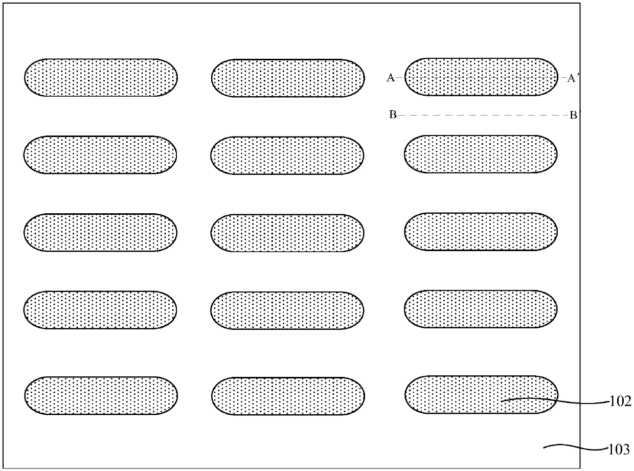
[0055] Such as Figure 1 to Figure 3 As shown, a semiconductor substrate 101 is provided, and an active region 102 and a shallow trench isolation structure 103 isolating the active region 102 are formed in the semiconductor substrate 101 . It should be noted that the method for forming the active region 102 and the shallow trench isolation structure 103 in this step is an existing method, so details will not be repeated here.

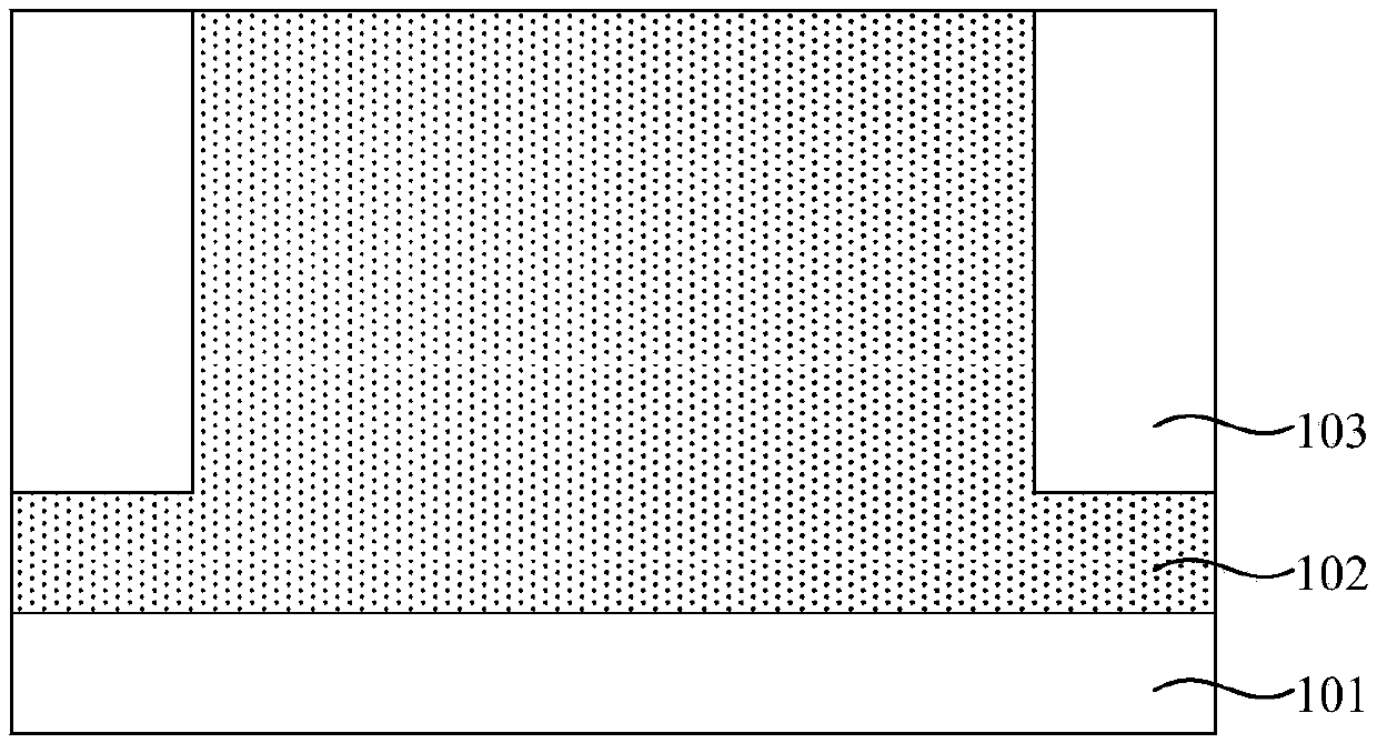
[0056] Such as Figure 4 to Figure 17 As shown, an active trench 112 is formed in the active region 102, and an isolation trench 114 is formed in the shallow trench isolation structure 103; the active trench 112 includes The front active trench 105 in 102, and the rear active trench 111 formed at the bottom of the front active trench 105, wherein the width of the rear active trench 111 is greater than that of the front active trench The width of the trench 105; the isolation trench 114 includes the front isolation trench 106 formed in the shallow tren...

Embodiment 2

[0088] The difference between this embodiment and Embodiment 1 is that in this embodiment, after the front-stage active trench 105 and the rear-stage active trench 111 are formed in the active region 102, the shallow trench A front isolation trench 06 and a rear isolation trench 113 are formed in the isolation structure 103 . The specific method is as follows: etching the active region 102 to form a front active trench 105 in the active region 102; and then etching the bottom of the front active trench 105 to form forming a rear active trench 111 at the bottom of the front active trench 105; and etching the shallow trench isolation structure 103 to form a front isolation trench 106 in the shallow trench isolation structure 103 and then etch the bottom of the front isolation trench 106 to form a rear isolation trench 113 at the bottom of the front isolation trench 106 ; It should be noted that the present embodiment differs from the first embodiment only in the formation seque...

Embodiment 3

[0090] Such as Figure 18 and Figure 19 As shown, this embodiment provides a buried gate structure manufactured by the method described in Embodiment 1 or Embodiment 2, and the buried gate structure includes:

[0091] A semiconductor substrate 101, an active region 102 and a shallow trench isolation structure 103 isolating the active region 102 are formed in the semiconductor substrate 101;

[0092] The active trench 112 includes the front active trench 105 formed in the active region 102, and the rear active trench 111 formed at the bottom of the front active trench 105, wherein the rear The width of the active trench 111 is greater than the width of the front active trench 105;

[0093] The isolation trench 114 includes the front isolation trench 106 formed in the shallow trench isolation structure 103, and the rear isolation trench 113 formed at the bottom of the front isolation trench 106, wherein the rear isolation trench The width of the groove 113 is greater than th...


PUM

PropertyMeasurementUnit
depthaaaaaaaaaa

Abstract

The invention provides an embedded gate structure and a manufacturing method thereof, and the method comprises the steps: providing a semiconductor substrate, and forming an active region and a shallow trench isolation structure for isolating the active region in the semiconductor substrate; forming an active trench in the active region and forming an isolation trench in the shallow trench isolation structure, wherein the active trench comprises a front-section active trench formed in the active region and a rear-section active trench formed at the bottom of the front-section active trench, and the width of the rear-section active trench is greater than that of the front-section active trench; the isolation trench comprises a front-section isolation trench formed in the shallow trench isolation structure and a rear-section isolation trench formed at the bottom of the front-section isolation trench, and the width of the rear-section isolation trench is greater than that of the front-section isolation trench; and forming a gate structure in the active trench and the isolation trench. According to the invention, the problem that the existing transistor cannot simultaneously consider the performance and the integration level is solved.

Description

technical field [0001] The invention relates to the field of semiconductor integrated circuits, in particular to a buried gate structure and a manufacturing method thereof. Background technique [0002] In the field of integrated circuit design, one way to improve circuit integration is to reduce the structural size of each device in the integrated circuit; and reducing the structural size of the device within a reasonable range can indeed improve the integration of the circuit, but when the structural size of the device is reduced To a certain extent, it will have adverse effects on the performance of the device. [0003] For transistors, when the structure size of the device is reduced to a certain extent, the length of the gate channel will be shortened, resulting in the short channel effect; therefore, when designing the transistor structure, in order to ensure the performance of the transistor, it is necessary to increase appropriately The structural size of the transi...

Claims


Application Information

Patent Timeline
Patent Type & Authority Applications(China)
IPC IPC(8): H01L29/423H01L21/28
CPCH01L29/42356H01L21/28008H01L29/4236
Inventor 不公告发明人
Owner CHANGXIN MEMORY TECH INC
Why Eureka
Try Eureka