
Vertical structure LED chip and preparation method thereof

A LED chip and vertical structure technology, applied in the direction of electrical components, circuits, semiconductor devices, etc., can solve the problems of high local heating, uneven electrical distribution, etc., and achieve the effects of prolonging service life, improving luminous intensity, and high luminous flux

Pending Publication Date: 2020-03-27
HEYUAN CHOICORE PHOTOELECTRIC TECH CO LTD
View PDF0 Cites 3 Cited by
  • Summary
  • Abstract
  • Description
  • Claims
  • Application Information

AI Technical Summary

Problems solved by technology

[0004] In order to overcome the deficiencies of the prior art, one of the objectives of the present invention is to provide a vertical structure LED chip, which can effectively solve the problem of excessive local heating caused by uneven electrical distribution, and is suitable for high-power LEDs.

Method used


Image

  • Vertical structure LED chip and preparation method thereof
  • Vertical structure LED chip and preparation method thereof
  • Vertical structure LED chip and preparation method thereof

Examples


Embodiment 1

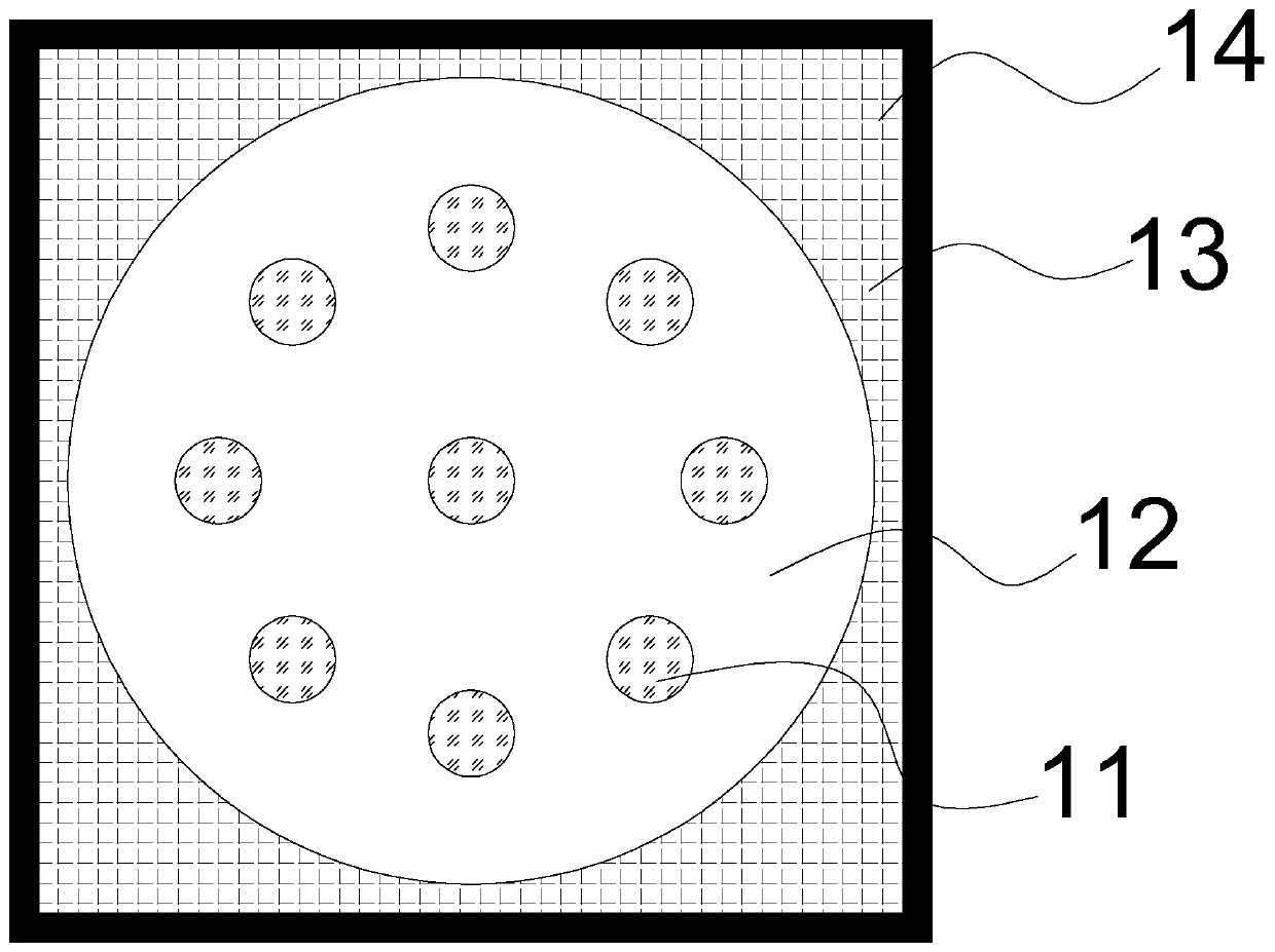
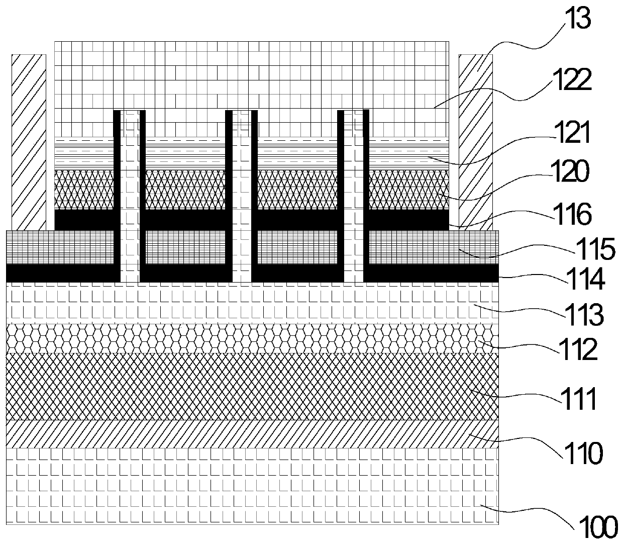
[0047] A kind of vertical structure LED chip, its longitudinal section structure is as follows figure 1 As shown, it includes a base layer and a circular light-emitting surface 12 arranged on the base layer and a P electrode 13 arranged on the outer edge of the circular light-emitting surface 12. The circular light-emitting surface 12 is coaxial with the P electrode 13; An insulating wall 14 is provided on the outside; a plurality of N electrode columns 11 are arranged inside the circular light emitting surface 12, and the plurality of N electrode columns 11 are distributed on the circular light emitting surface 12 in the form of a ring or a polygon, centrally or axisymmetrically. Among them, the bottom end of the N electrode column 11 is electrically connected to the base layer, and the top end is electrically connected to the circular light emitting surface 12 .

[0048] Such as figure 2 As shown, wherein the circular light-emitting surface 12 includes LED epitaxial layers...

Embodiment 2

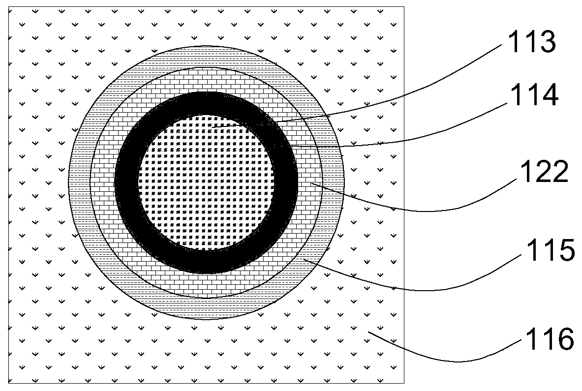
[0051] A vertical structure LED chip, such as Figure 1-Figure 3 As shown, it includes a base layer, a circular light-emitting surface 12 arranged on the base layer, and a P electrode 13 arranged on the outer edge of the circular light-emitting surface 12. The circular light-emitting surface 12 is concentric with the P electrode 13; the peripheral device of the P electrode 13 There is an insulating wall 14; the circular light-emitting surface 12 is a 35mil×35mil LED chip, and a plurality of 9 electrode columns are arranged inside, one of the plurality of N electrode columns 11 is located at the center point, and the other 8 are arranged in a circular array around the center point Distributed in the circular light emitting surface 12 , the bottom end of the N electrode column 11 is electrically connected to the base layer, and the top end is electrically connected to the circular light emitting surface 12 .

[0052] Among them, the circular light-emitting surface 12 includes an...

Embodiment 3

[0075] A vertical structure LED chip, such as Figure 4 As shown, it includes a base layer, a circular light-emitting surface 12 arranged on the base layer, and a P electrode 13 arranged on the outer edge of the circular light-emitting surface 12. The circular light-emitting surface 12 is concentric with the P electrode 13; the peripheral device of the P electrode 13 There is an insulating wall 14; the circular light-emitting surface 12 is a 35mil×35mil LED chip, and 14 N electrode columns 11 are arranged inside, and the 14 N electrode columns 11 are adjacent to each other in a diamond shape, and the circular light-emitting surface 12 is symmetrically distributed in the center In the circular light emitting surface 12 , the bottom end of the N electrode post 11 is electrically connected to the base layer, and the top end is electrically connected to the circular light emitting surface 12 .

[0076] Among them, the circular light-emitting surface 12 includes an LED epitaxial la...


PUM

PropertyMeasurementUnit
thicknessaaaaaaaaaa
thicknessaaaaaaaaaa
thicknessaaaaaaaaaa

Abstract

The invention discloses a vertical structure LED chip. According to the chip, a circular light-emitting surface is adopted on a rectangular substrate, wherein a plurality of N electrode columns are arranged in the circular light-emitting surface, the N electrode columns are distributed in the circular light-emitting surface in an annular or polygonal mode, in a central symmetry mode or in an axialsymmetry mode, the bottom ends of the N electrode columns are electrically connected with the substrate layer, the top ends of the N electrode columns are electrically connected with the circular light-emitting surface, and the N electrode columns are integrally formed by an N electrode layer of the substrate layer. The LED chip with the vertical structure effectively solves the problems of non-uniform luminous intensity, over-high local temperature and the like caused by non-uniform current density in a luminous surface, and a manufactured LED product has better stability and durability.

Description

technical field [0001] The invention relates to the technical field of semiconductors, in particular to the field of LED chips, in particular to a vertical structure LED chip and a preparation method thereof. Background technique [0002] At present, light emitting diodes (Light Emitting Diode, LED) have been widely used in application fields such as indoor and outdoor lighting, outdoor lighting, vehicle lights, and hand-held lighting. Light Emitting Diode (LED) is a device that converts electrical energy into light energy by PN junction. It has the advantages of good controllability, fast start-up, long life, high luminous efficiency, safety, energy saving and environmental protection, etc. Profound changes in the industry, while also leading the innovation in the display field. [0003] With the development of the LED industry, high-power LEDs are becoming more and more popular. With the increase of the power used, the current injected per unit area is also required to b...

Claims


Application Information

Patent Timeline
Patent Type & Authority Applications(China)
IPC IPC(8): H01L33/24H01L33/38H01L33/00
CPCH01L33/24H01L33/387H01L33/007
Inventor 李国强
Owner HEYUAN CHOICORE PHOTOELECTRIC TECH CO LTD
Learn More