Photoresist spin-coating device and photoresist spin-coating method

A rotary drive device and photoresist technology, applied in optics, photomechanical equipment, photoplate making process coating equipment, etc., can solve the problems of reducing device manufacturing yield and productivity, poor surface uniformity of photoresist layer, and increasing manufacturing costs, etc. , to eliminate the effect of turbulence and reduce the effect

Pending Publication Date: 2020-03-31
CHANGXIN MEMORY TECH INC
View PDF10 Cites 2 Cited by
  • Summary
  • Abstract
  • Description
  • Claims
  • Application Information

AI Technical Summary

Problems solved by technology

As the size of the wafer increases and the rotational speed of the wafer increases, the impact of turbulence on the photoresist layer becomes greater and greater, forming image 3 Wrinkles shown, i.e. the surface uniformity of the photoresist layer is getting worse
[0005] The above-mentioned rough structure is not conducive to the growth of subsequent functional layers, which reduces the device manufacturing yield and productivity, thereby increasing the manufacturing cost

Method used


Image

  • Photoresist spin-coating device and photoresist spin-coating method
  • Photoresist spin-coating device and photoresist spin-coating method
  • Photoresist spin-coating device and photoresist spin-coating method

Examples


Embodiment 1

[0061] This embodiment describes the photoresist spin coating device of the present invention.

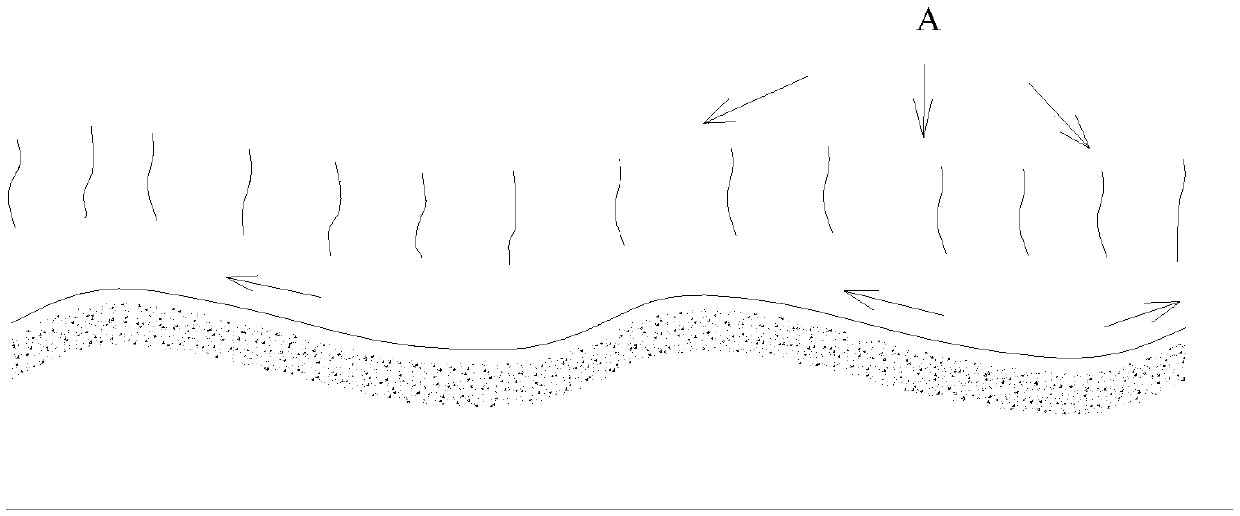
[0062] Such as Figure 4 As shown, the photoresist spin coating device 100 of this embodiment includes: a rotary drive device 10; a wafer tray 70 located on the rotary drive device 10; and a cover plate 50 located on the wafer tray, the cover plate and the wafer The tray is driven to rotate by the rotary drive device 10 .

[0063] The rotation driving device 10 drives the wafer tray 70 to rotate by the first rotation axis. The wafer tray 70 is used to place a wafer 80 .

[0064] Such as Figure 4 As shown, an inner chamber 40 is disposed around the wafer tray 70 . The lower part of the outer end of the inner cavity body 40 is provided with a liquid discharge port 30 . An outer cavity 20 is disposed outside the inner cavity 40 . The lower part of the outer cavity 20 is provided with a liquid outlet (not shown). Optionally, upper parts of the inner cavity 40 and the outer cavi...

Embodiment 2

[0072] see Figure 7 , this embodiment provides a flowchart of a method for manufacturing a photoresist layer. The photoresist spin coating device 100 comprises a rotary drive device 10; a wafer tray 70 positioned on the rotary drive device 10; and a cover plate 50 positioned on the wafer tray, the cover plate 50 and the wafer tray 70 are driven by the rotation The device 10 is driven in rotation.

[0073] The photoresist spin coating method of the photoresist spin coating device 100 includes the following steps:

[0074] placing the wafer 80 on the wafer tray 70;

[0075] The photoresist layer is spin-coated on the surface of the wafer 80 by using a shower head (not shown);

[0076] Reflow the photoresist layer;

[0077] Closing the cover plate 50 so that it covers the wafer 80;

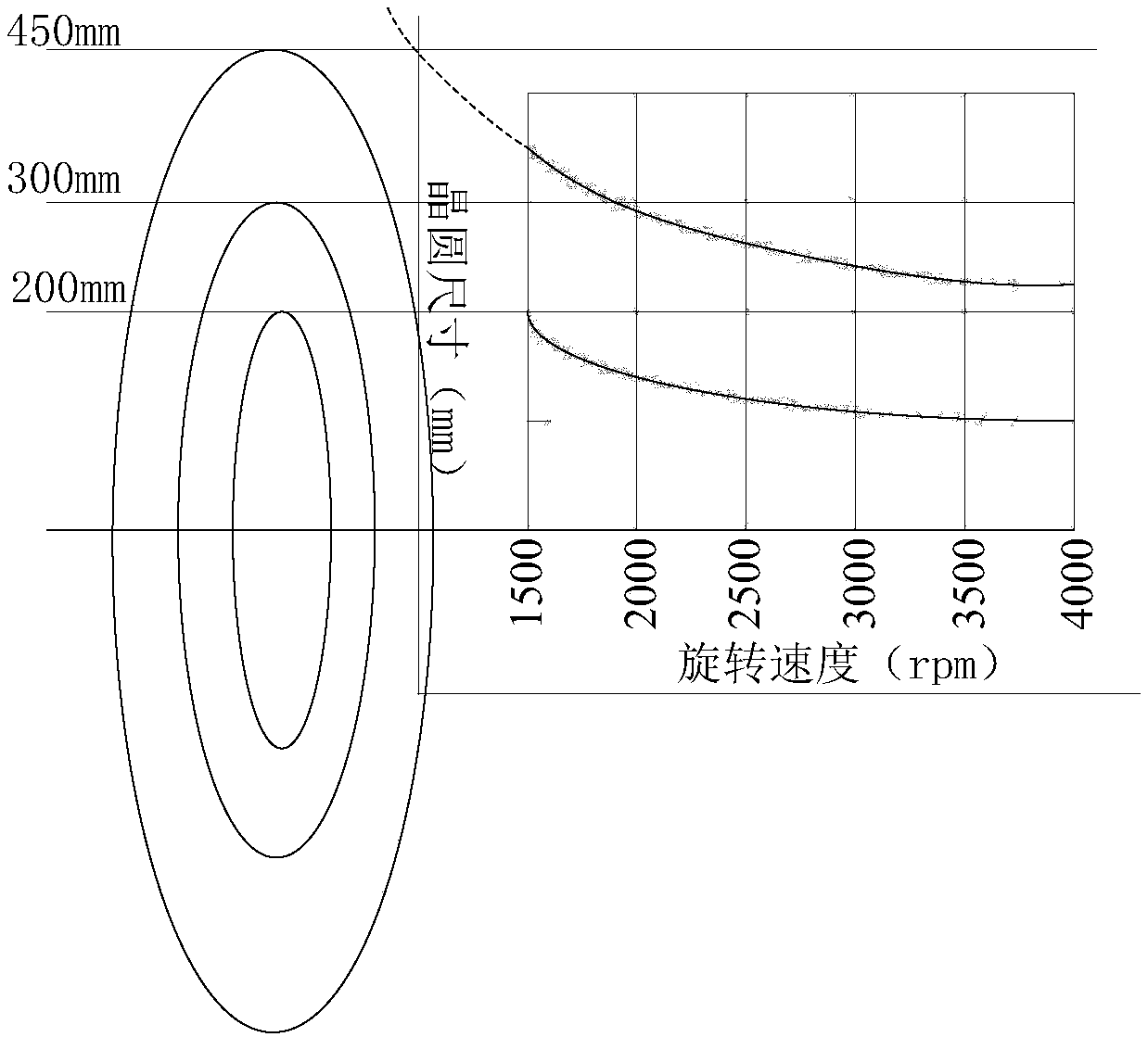
[0078] The wafer tray 70 is driven by the rotary driving device 10 to drive the wafer 80 to rotate; the rotation speed is 500-5000 rpm (500-5000 rpm). Optionally, the rotation speed of the waf...


PUM

PropertyMeasurementUnit
diameteraaaaaaaaaa

Abstract

The invention provides a photoresist spin-coating method and a photoresist spin-coating device. The photoresist spin-coating device comprises a rotation driving device; a wafer tray positioned above the rotation driving device; and a cover plate positioned on the wafer tray. The cover plate and the wafer tray are driven to rotate by a rotating device. A cover plate is arranged on an inner cavity and the wafer tray. During execution of the photoresist spin-coating process, the cover plate is closed and opened before and after a main rotation stage of spin-coating photoresist layer film formation, so that the turbulence influence of airflow flowing on a photoresist layer during main rotation can be effectively reduced, the uniformity of the thickness of the photoresist layer is improved, productivity is improved, and manufacturing cost is reduced.

Description

technical field [0001] The invention relates to a semiconductor manufacturing process and a manufacturing device, in particular to a photoresist spin-coating device and a photoresist spin-coating method. Background technique [0002] In order to form various functional layers on the wafer, it is usually necessary to spin-coat photoresist after forming the functional layers on the wafer, and form the desired functional layer pattern by means of exposure, development and etching. [0003] However, with the development of high integration and high speed of large-scale integrated circuits, and with the increase of wafer size, during the manufacturing process of wafers with a size of 8 inches and above, when using photoresist for spin coating , which usually results in uneven rough patterns on the surface of the spin-coated photoresist layer, such as figure 1 As shown, for example, a method for patterning a functional layer is disclosed in the prior art, which includes spin-coat...

Claims


Application Information

Patent Timeline
Patent Type & Authority Applications(China)
IPC IPC(8): G03F7/16
CPCG03F7/162G03F7/168
Inventor 黄帅
Owner CHANGXIN MEMORY TECH INC
Why Eureka
Try Eureka