
Display panel and driving method

A technology for display panels and driving methods, applied to static indicators, instruments, etc., can solve problems such as high current, decreased screen contrast, and impact on the image quality of micro-light-emitting diode displays

Active Publication Date: 2020-04-03
INTERFACE TECH CHENGDU CO LTD +2
View PDF9 Cites 2 Cited by
  • Summary
  • Abstract
  • Description
  • Claims
  • Application Information

AI Technical Summary

Problems solved by technology

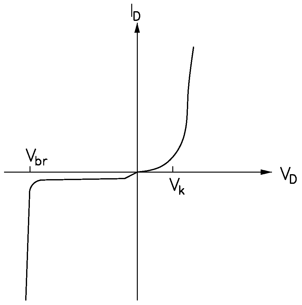
[0004] Although the reverse bias current is extremely small, the number of micro LEDs on the display panel is large, and the reverse bias current direction of each micro LED is the same. After accumulation, a large sum of reverse bias currents can be formed. The sum of the bias currents will affect the picture quality of the micro-LED display, resulting in a decrease in picture contrast
Furthermore, when the anode voltage of the LED is lower than the cathode voltage and the voltage difference between the anode and the cathode is greater than the breakdown voltage of the LED, a large current will be generated instantly causing the LED to burn out

Method used


Image

  • Display panel and driving method
  • Display panel and driving method
  • Display panel and driving method

Examples


Embodiment 1

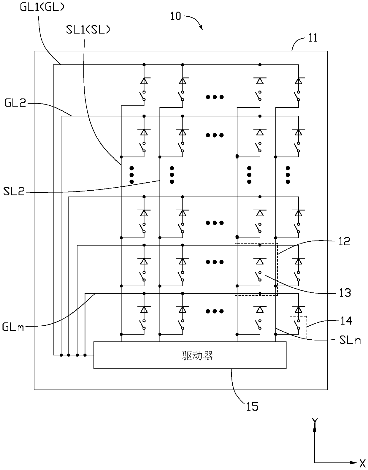
[0047] see figure 1 The display panel 10 provided in this embodiment includes a substrate 11, m gate lines (GL1˜GLm, m>2) and n data lines (SL1˜SLn, n>2) formed on the substrate 11, each The gate lines are arranged in parallel with each other at intervals, and the data lines are arranged in parallel with each other. The m gate lines and the n data lines are insulated from each other and cross each other to define a plurality of sub-pixels 12 arranged in an array, such as figure 1 As shown in , the X direction is defined as the row direction of the array, and the Y direction is defined as the column direction of the array.

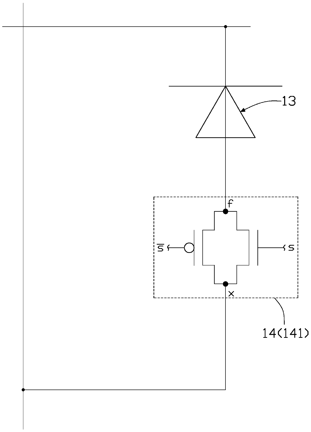
[0048] read on figure 1 , the display panel 10 further includes a plurality of LEDs 13 disposed on the substrate 11 , and each LED 13 is located in a sub-pixel 12 . Each light emitting diode 13 has an anode and a cathode, the anode of each light emitting diode 13 is electrically connected to the gate line GL defining the sub-pixel 12 where it is located, ...

Embodiment 2

[0066] see Figure 5 The difference between the display panel 20 provided in this embodiment and the first embodiment mainly lies in that the circuit structure of the protection circuit 24 in this embodiment is different from that of the protection circuit 14 in the first embodiment.

[0067] In this embodiment, each protection circuit 24 includes a first switch unit 241 and a second switch unit 242 . Wherein, the first switch unit 241 is respectively electrically connected to the anode of the light emitting diode 23 and the gate line GL to which the light emitting diode 23 is electrically connected; Connect the data line SL.

[0068] read on Figure 5 , in this embodiment, the driver 25 is used to output a control signal to each protection circuit 24 to control each protection circuit 24 itself to be turned on or open, so as to control each light emitting diode 23 electrically connected to each protection circuit 24 to be kept on or short-circuited. state.

[0069] see ...

Embodiment 3

[0074] see Figure 7 The difference between the display panel 30 provided in this embodiment and the second embodiment mainly lies in that the circuit structure of the protection circuit 34 in this embodiment is different from that of the protection circuit 24 in the second embodiment.

[0075] In this embodiment, each protection circuit 34 includes a first switch unit 341 and a resistance element 342 . Wherein, the circuit structure and connection mode of the first switch unit 341 are basically the same as those of the first switch unit 241 in the second embodiment, and will not be repeated here. The resistor element 342 is respectively electrically connected to the anode of the light emitting diode 33 and the data line SL to which the light emitting diode 33 is electrically connected.

[0076] read on Figure 7 , in this embodiment, the driver 35 is used to output a control signal to each protection circuit 34 to control each protection circuit 34 itself to be turned on or...


PUM


Abstract

The embodiment of the invention provides a display panel. The display panel comprises m gate lines which are arranged at intervals along a first direction; n data lines, arranged at intervals in the second direction, and the m gate lines and the n data lines being insulated and crossed to define a plurality of sub-pixels; a plurality of light-emitting diodes, each light-emitting diode being formedin a sub-pixel, each light-emitting diode being electrically connected to a data line and a gate line defining the sub-pixel where the light-emitting diode is located; a plurality of protection circuits, electrically connected with the plurality of light-emitting diodes in a one-to-one correspondence manner, and each protection circuit being used for carrying out overcurrent protection when the electrically connected light-emitting diode is in a non-working state; and a driver, electrically connected with the m gate lines, the n data lines and the plurality of protection circuits and being used for outputting a control signal to the protection circuits according to the working state of the light emitting diode so as to switch the electric connection relationship between the protection circuits and the light emitting diode. The embodiment of the invention further provides a driving method.

Description

technical field [0001] The present invention relates to the technical field of image display, in particular to a display panel and a driving method applied to the display panel. Background technique [0002] In the prior art, a micro light emitting diode display defines a plurality of pixel areas arranged in an array on the display panel, each pixel area includes a plurality of sub-pixels, each sub pixel is provided with a micro light emitting diode, and a driving signal is output through a driver To each micro-light emitting diode, each micro-light-emitting diode can be controlled to light up or turn off, and through the light-emitting coordination of each micro-light-emitting diode, the micro-light-emitting diode display can display different images. [0003] Among them, the micro light emitting diode has the characteristics of "forward conduction and reverse cut off", that is, if the anode voltage of the micro light emitting diode is higher than the negative voltage and t...

Claims


Application Information

Patent Timeline
IPC IPC(8): G09G3/32
CPCG09G3/32
Inventor 陈忠君汪忠辉庄胜钧陈伯纶
Owner INTERFACE TECH CHENGDU CO LTD
Learn More