Trench isolation structure and forming method thereof, and semiconductor device and forming method thereof

A trench isolation and semiconductor technology, which is applied in semiconductor devices, semiconductor/solid-state device manufacturing, electric solid-state devices, etc., can solve the problems of decreased storage performance of integrated circuit memory, poor storage capacity of integrated circuit memory, etc., to improve storage performance, The effect of increasing the equivalent resistance and reducing the area

Pending Publication Date: 2020-04-07
CHANGXIN MEMORY TECH INC
View PDF0 Cites 2 Cited by
  • Summary
  • Abstract
  • Description
  • Claims
  • Application Information

AI Technical Summary

Problems solved by technology

[0002] At present, the existing integrated circuit memory can usually include several transistors. In order to reduce the area of ​​the integrated circuit memory to achieve the maximum integration, a trench type transistor structure is usually used. When the trench type transistor structure is used, the trench A leakage region is formed between the trench isolation structure and the gate structure of the storage transistor, and electrons between the source and drain regions of the storage transistor may migrate into the leakage region, thereby generating a leakage current, resulting in a decrease in the storage performance of the integrated circuit memory, And the larger the area of ​​the leakage area, the smaller the equivalent resistance on the leakage path, the greater the leakage current will be, and the worse the storage capacity of the integrated circuit memory is, how to reduce the leakage current has become an urgent problem to be solved

Method used


Image

  • Trench isolation structure and forming method thereof, and semiconductor device and forming method thereof
  • Trench isolation structure and forming method thereof, and semiconductor device and forming method thereof
  • Trench isolation structure and forming method thereof, and semiconductor device and forming method thereof

Examples


Embodiment Construction

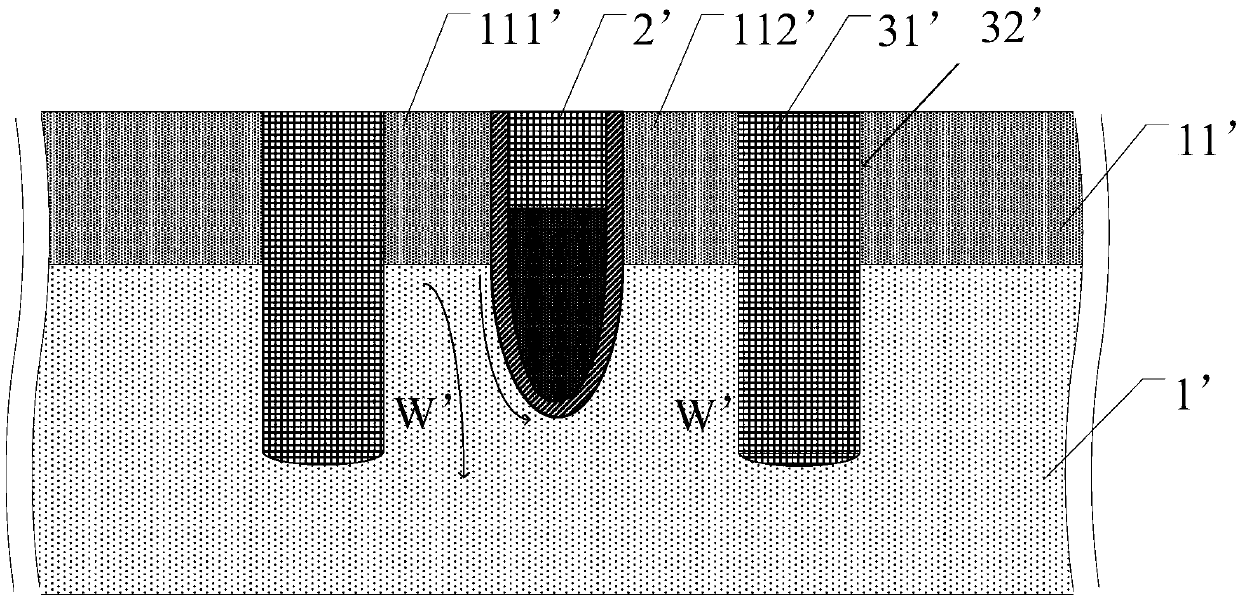
[0055] figure 1 It is a semiconductor device, which includes a substrate 1' and a trench isolation structure formed in the substrate 1', the trench isolation structure is used to define an active region 11', and the trench isolation structure Including an isolation material layer 31' formed in an isolation trench 32', a drain region 111', a source region 112' and a gate structure 2' are formed in each of the active regions 11', and the gate structure 2 'located between the drain region 111' and the source region 112' to form a storage transistor. Such as figure 1 As shown, the trench isolation structure extends from the top surface of the substrate 1' to the inside of the substrate 1', and the lateral width of the entire trench isolation structure is approximately the same, resulting in the trench The area of ​​the leakage region W' between the isolation structure and the gate structure 2' is very large. When the storage transistor is in use, electrons migrate from the drain...


PUM


Abstract

The invention provides a trench isolation structure and a forming method thereof, and a semiconductor device and a forming method thereof. The forming method of the trench isolation structure comprises the following steps: forming a trench isolation structure in a substrate, and defining an active region through the trench isolation structure, wherein the trench isolation structure is provided with a first isolation part and a second isolation part which are connected with each other, the second isolation part is located below the first isolation part, and the transverse width of the second isolation part in the direction perpendicular to the height direction is larger than the transverse width of the first isolation part in the direction perpendicular to the height direction, so that thesecond isolation part is enabled to protrude transversely relative to the first isolation part, so that the area of a leakage region is reduced, the equivalent resistance on a leakage path is increased, a leakage current is reduced, and the storage performance of the semiconductor device is improved.

Description

technical field [0001] The invention relates to the field of semiconductor manufacturing, in particular to a trench isolation structure and a forming method thereof, a semiconductor device and a forming method thereof. Background technique [0002] At present, the existing integrated circuit memory can usually include several transistors. In order to reduce the area of ​​the integrated circuit memory to achieve the maximum integration, a trench type transistor structure is usually used. When the trench type transistor structure is used, the trench A leakage region is formed between the trench isolation structure and the gate structure of the storage transistor, and electrons between the source and drain regions of the storage transistor may migrate into the leakage region, thereby generating a leakage current, resulting in a decrease in the storage performance of the integrated circuit memory, Moreover, the larger the area of ​​the leakage region, the smaller the equivalent ...

Claims


Application Information

Patent Timeline
Patent Type & Authority Applications(China)
IPC IPC(8): H01L21/762H01L27/105H01L21/8239
CPCH01L21/76224H01L27/105H10B99/00
Inventor 林仕杰江文湧
Owner CHANGXIN MEMORY TECH INC
Why Eureka
Try Eureka