Method for manufacturing LED transparent display screen and display screen

A transparent display screen and LED device technology, applied in static indicators, instruments, identification devices, etc., can solve the problems of high failure rate and low production efficiency, meet the requirements of reducing operating space, improve production efficiency, and improve LED stickiness. The effect of bonding strength

Active Publication Date: 2020-04-17
湖南创瑾科技有限公司
View PDF13 Cites 0 Cited by
  • Summary
  • Abstract
  • Description
  • Claims
  • Application Information

AI Technical Summary

Problems solved by technology

For this reason, the present invention proposes a method for manufacturing LED transparent display screens, the process of the method for manufacturing LED transparent display screens is simple, and the problems of low production efficiency and high failure rate are solved

Method used

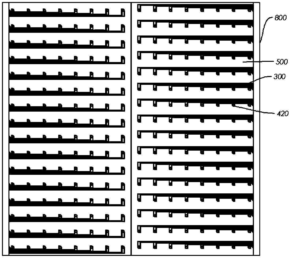
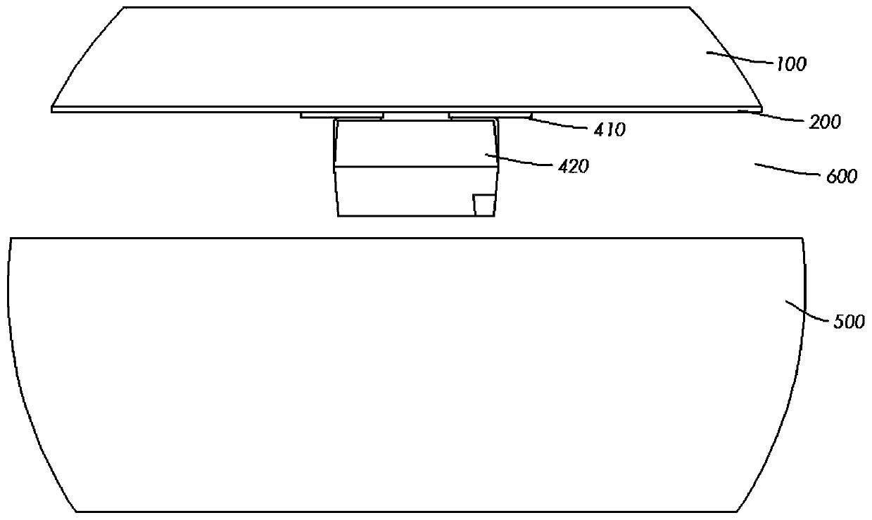

Image

  • Method for manufacturing LED transparent display screen and display screen
  • Method for manufacturing LED transparent display screen and display screen
  • Method for manufacturing LED transparent display screen and display screen

Examples


Embodiment Construction

[0033] Embodiments of the present invention are described in detail below, examples of which are shown in the drawings, wherein the same or similar reference numerals designate the same or similar elements or elements having the same or similar functions throughout. The embodiments described below by referring to the figures are exemplary only for explaining the present invention and should not be construed as limiting the present invention.

[0034] In the description of the present invention, if there are descriptions of first, second, third, fourth, etc., it is only for the purpose of distinguishing technical features, and it cannot be understood as indicating or implying relative importance or implicitly indicating the indicated The number of technical features or implicitly indicates the sequence of the indicated technical features.

[0035] In the description of the present invention, unless otherwise clearly defined, terms such as setting and connecting should be unders...


PUM


Abstract

The invention discloses a method for manufacturing an LED transparent display screen. The method comprises the following steps: coating a transparent conductive layer on a transparent substrate; performing vacuum sputtering on the transparent conductive layer by using a mask plate to form a bonding pad; etching a driving electrode on the transparent conductive layer, wherein one end of the drivingelectrode is connected with the bonding pad; coating solder paste on the bonding pad in a printing manner; fixing the LED device on the bonding pad through solder paste; crimping the other end of thedriving electrode to a driving circuit board; and bonding the transparent substrate with the transparent front protection panel by using a transparent non-conductive optical adhesive. The bonding pads are formed through vacuum sputtering; compared with a traditional mode, the bonding pads are smoother, one forming capacity of the multiple bonding pads is achieved, batch vacuum sputtering can be conducted on the bonding pads of any number and any shape through cooperation with the mask plate, and the production efficiency is greatly improved; the solder paste is coated in a printing mode, so that the solder paste coating efficiency is improved. In addition, by means of the means, the requirement for the operation space is lowered, and the pixel density is further improved.

Description

technical field [0001] The invention belongs to the field of transparent display screens, and in particular relates to a method for manufacturing a LED transparent display screen and the display screen. Background technique [0002] In recent years, the LED display application industry has developed steadily, and its overall scale has been increasing year by year. At present, it has become an important part of the LED industry chain. LED display application products represented by LED displays have been widely used in various fields of social economy. Driven by the application market, LED transparent display has become a hot spot in current research. It can enrich visual content without blocking the line of sight. There are a large number of applications in exhibition halls, museums, science and technology museums and other places. [0003] At present, the manufacturing method of LED transparent display screen is as follows: firstly, the transparent conductive layer is coat...

Claims


Application Information

Patent Timeline
Patent Type & Authority Applications(China)
IPC IPC(8): G09F9/33G09G3/32
CPCG09F9/33G09G3/32
Inventor 陈剑卿赖金洪周佩先
Owner 湖南创瑾科技有限公司
Why Eureka
Try Eureka