Semiconductor laser, semiconductor laser refrigeration structure and manufacturing method thereof

A technology of lasers and semiconductors, applied in the direction of semiconductor lasers, lasers, laser components, etc., can solve the problems of semiconductor lasers such as poor sealing

Inactive Publication Date: 2020-04-28
SUZHOU EVERBRIGHT PHOTONICS CO LTD
View PDF7 Cites 1 Cited by
  • Summary
  • Abstract
  • Description
  • Claims
  • Application Information

AI Technical Summary

Problems solved by technology

[0003] In view of this, an embodiment of the present invention provides a semiconductor laser, a semiconductor laser refrigeration structure and a manufacturing method thereof, to solve the problem of poor sealing between semiconductor lasers when a plurality of semiconductor lasers form a semiconductor laser array

Method used


Image

  • Semiconductor laser, semiconductor laser refrigeration structure and manufacturing method thereof
  • Semiconductor laser, semiconductor laser refrigeration structure and manufacturing method thereof
  • Semiconductor laser, semiconductor laser refrigeration structure and manufacturing method thereof

Examples


Embodiment Construction

[0025] In order to make the purpose, technical solutions and advantages of the embodiments of the present invention clearer, the technical solutions in the embodiments of the present invention will be clearly and completely described below in conjunction with the drawings in the embodiments of the present invention. Obviously, the described embodiments It is a part of embodiments of the present invention, but not all embodiments. Based on the embodiments of the present invention, all other embodiments obtained by those skilled in the art without creative efforts fall within the protection scope of the present invention.

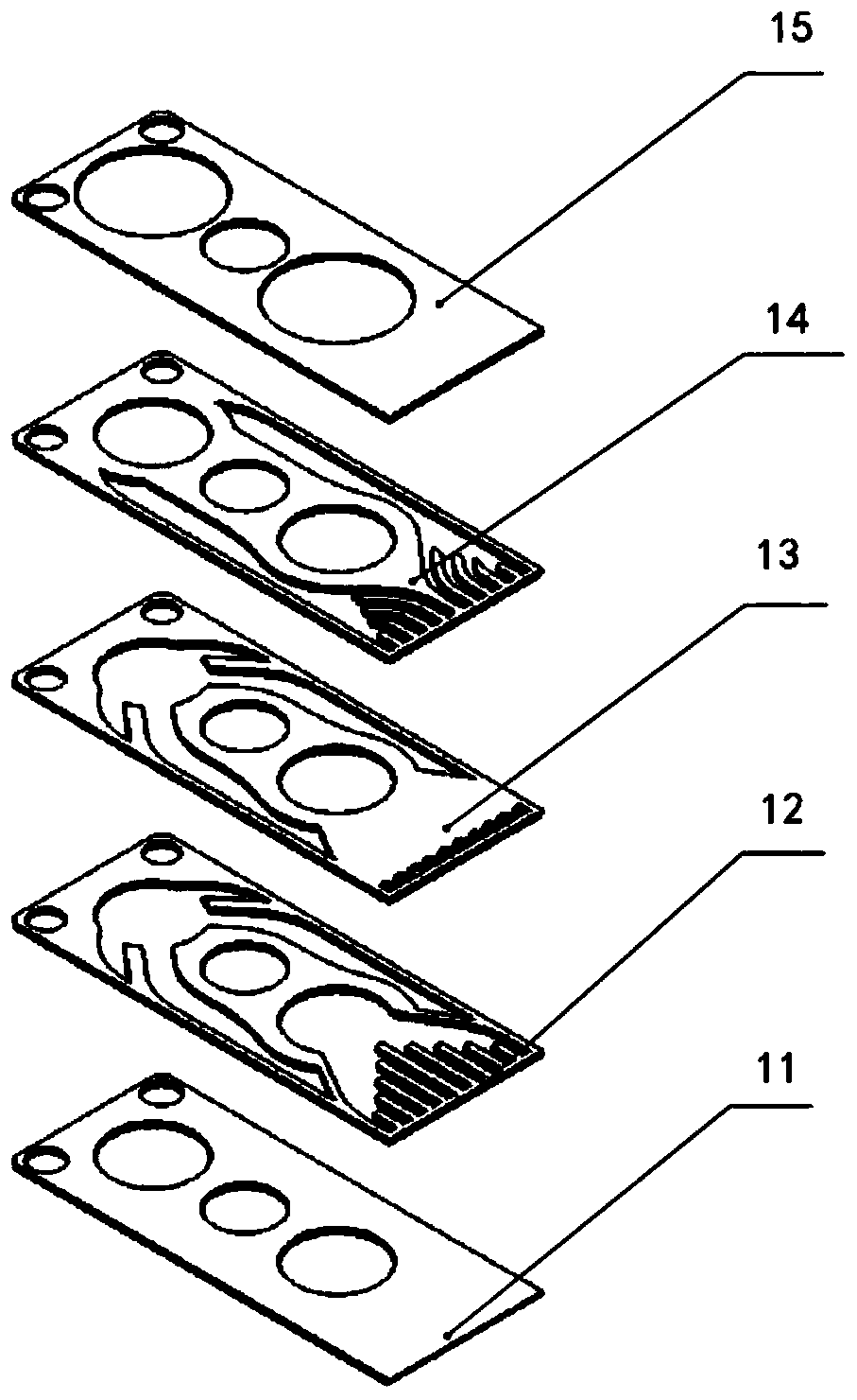
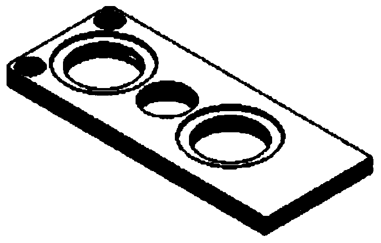
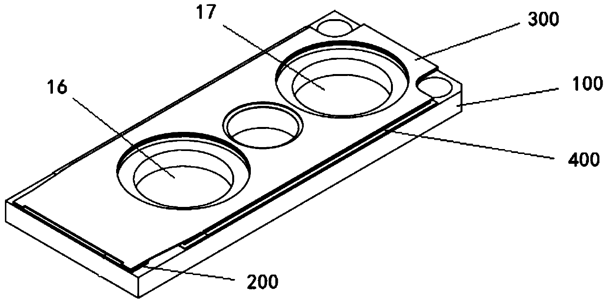
[0026] An embodiment of the present invention provides a semiconductor laser cooling structure, such as Figure 4 As shown, it includes a lower cover sheet 1, a water return sheet 2, a water distribution sheet 3, a microchannel heat sink 4, and an upper cover sheet 5 arranged sequentially from bottom to top. The upper cover sheet 5 includes: an insulating lay...


PUM


Abstract

The invention discloses a semiconductor laser, a semiconductor laser refrigeration structure and a manufacturing method of the semiconductor laser refrigeration structure. The semiconductor laser refrigeration structure comprises a lower cover piece, a water return piece, a water diversion piece, a micro-channel cooling fin and an upper cover piece which are sequentially arranged from bottom to top, wherein the upper cover piece comprises an insulating layer, a first step metal layer and a second step metal layer; the first step metal layer is arranged on the insulating layer; the second stepmetal layer is arranged on the insulating layer; the lower cover piece, the water return piece, the water diversion piece, the micro-channel cooling fin, the insulating layer and the second step metallayer are respectively provided with coaxial cooling water channels, and the peripheries of the cooling water channels are sealed by welding; the length of the upper cover piece is less than that ofthe micro-channel cooling fin, and the thickness of the second step metal layer is greater than that of the first step metal layer. According to the semiconductor laser adopting the semiconductor laser refrigeration structure, each semiconductor laser can be connected in a sealed welding mode to form a semiconductor laser array, and strict sealing among all the semiconductor lasers is achieved.

Description

technical field [0001] The invention relates to the technical field of semiconductor lasers, in particular to a semiconductor laser, a semiconductor laser cooling structure and a manufacturing method thereof. Background technique [0002] Since the semiconductor laser needs to dissipate heat when it is working, water is often used inside the semiconductor laser to dissipate heat from the semiconductor laser. The cooling structure of the semiconductor laser is as follows: figure 1 As shown in -2, it is a modular copper microchannel cooler with a 5-layer structure, including a lower cover sheet 11, a water return sheet 12, a water distribution sheet 13, a microchannel cooling sheet 14, and an upper Cover slip 15. Semiconductor lasers such as image 3 As shown, it includes a semiconductor laser cooling structure 100, a light-emitting unit 200, an insulating layer 400, and a cathode sheet 300. The semiconductor laser cooling structure includes a water inlet hole 16 and a water...

Claims


Application Information

Patent Timeline
Patent Type & Authority Applications(China)
IPC IPC(8): H01S5/024H01S5/022
CPCH01S5/022H01S5/02423
Inventor 潘华东靳嫣然周立王俊闵大勇廖新胜
Owner SUZHOU EVERBRIGHT PHOTONICS CO LTD
Why Eureka
Try Eureka