
Eureka
For R&D, Eureka makes reading and utilizing patents & technical documents easy.
Eureka AIR
Designed for self-driven R&D workflows. Generate viable solutions, solve complex R&D challenges, empower your innovation with AI.

Eureka Materials
Designed for material experts only. Revolutionize your material R&D, from search, analyze, to developing new materials.

TechResearch
Generate reliable direction feasibility study reports for your R&D in just a few steps.

TechSeek
Discover and master advanced knowledge NOW. Basics, ideas, possibilities, all at once.

TechMind
As an expert in R&D Theories, TechMind can generates customized viable solutions instantly.

TechRisk
Analyze your overall solution with one click, know your potential R&D risks in advance.

TechMonitor
Get weekly tech updates, stay abreast of the latest tech innovations and key insights.
Batch transfer method of micro-elements
A transfer method and micro-component technology, which is applied in the manufacture of electrical components, semiconductor devices, semiconductor/solid-state devices, etc., can solve the problems of large growth density and huge transfer quantity, and achieve high transfer efficiency, simple transfer equipment, and difficult transfer process low effect
- Summary
- Abstract
- Description
- Claims
- Application Information
AI Technical Summary
Problems solved by technology
Method used
Image

Examples
Embodiment Construction
[0032] In order to make the purpose, technical solution and effect of the present application more clear and definite, the present application will be further described in detail below with reference to the accompanying drawings and examples.
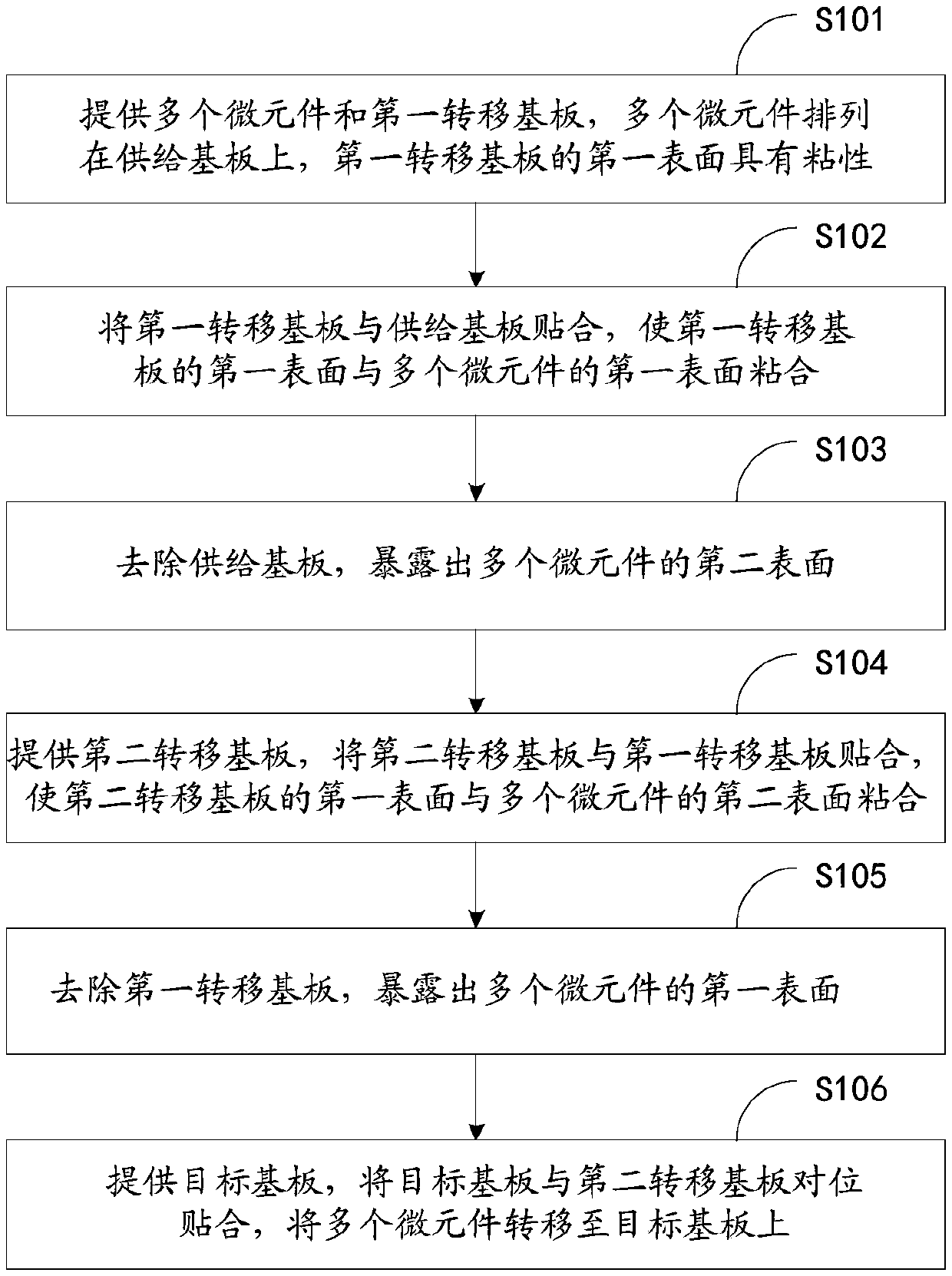
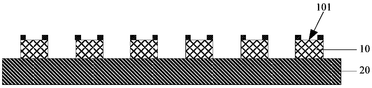
[0033] The present application provides a method for transferring micro components in batches, using two transfer substrates as transfer equipment, and transferring the micro components to the target substrate in two steps. In this way, the entire transfer process does not require the use of transfer heads and complicated transfer equipment, which greatly simplifies the difficulty of transfer. The batch transfer method disclosed in this application can be used to transfer micro-light-emitting diode devices (Micro-LED). Here, the transfer of Micro-LED is taken as an example for illustration, but it is not limited to this device, and can also be used for transfer of other micro components.
[0034] see figure 1 , figure 1 It is a schema...
PUM
 Abstract
Description
Claims
Application Information
 - R&D Engineer
- R&D Manager
- IP Professional
- Industry Leading Data Capabilities
- Powerful AI technology
- Patent DNA Extraction
Browse by: Latest US Patents, China's latest patents, Technical Efficacy Thesaurus, Application Domain, Technology Topic, Popular Technical Reports.
© 2024 PatSnap. All rights reserved.Legal|Privacy policy|Modern Slavery Act Transparency Statement|Sitemap|About US| Contact US: help@patsnap.com