Management system for semiconductor manufacturing equipment

a management system and semiconductor technology, applied in the field of management systems for semiconductor manufacturing equipment, can solve the problems of long production lags, complex engineering endeavors, and difficulty in effectively monitoring the progress of various silicon wafers through the manufacturing process, so as to improve overall productivity, optimize the movement of wafers, and enhance transfer efficiency and speed

Inactive Publication Date: 2007-04-26
SAMSUNG ELECTRONICS CO LTD
View PDF14 Cites 29 Cited by
  • Summary
  • Abstract
  • Description
  • Claims
  • Application Information

AI Technical Summary

Benefits of technology

[0015] Embodiments of the invention provide a management system for semiconductor manufacturing equipment capable of enhancing transfer efficiency and speed for wafer cassettes throughout a manufacturing process. Embodiments of the invention also allow definitive location and status information to be obtained in real-time, thereby optimizing wafer movement throughout the manufacturing process. These improvements increase overall productivity.

Problems solved by technology

Accordingly, the physical transfer (e.g., process flow, holding and storage, etc.) of the silicon wafers through the production facility—in order to receive application of the proper sequence of processes—is a very complex engineering endeavor.
Indeed, the inevitable breakdown or maintenance down-time associated with a single piece of fabrication equipment may result in lengthy production lags for numerous wafers, unless the breakdown is quickly identified and remedied.
However, the largely automated nature of the production facility's equipment and the vast area occupied by this equipment in huge factory facilities make it difficult to effectively monitor the progress of various silicon wafers through the manufacturing process.
However, this type of wafer management system suffers from several problems.
Thus, centralized optimization of the overall process is impossible as no control, and little visibility is possible over the non-automated process steps.
As a result, the transfer efficiency and speed for wafer cassettes between different pieces of semiconductor manufacturing equipment are impossible to optimize.
Additionally, while the arrival and departure of cassettes may be tracked in point by point fashion, the conventional system offers no real-time mechanism for tracking actual movement (or lack of movement) by cassettes through the manufacturing process.
This approach can require a great deal of time and precludes a real-time understanding of a particular wafer's processing status.
All of these problems adversely effect productivity.

Method used


Image

  • Management system for semiconductor manufacturing equipment
  • Management system for semiconductor manufacturing equipment
  • Management system for semiconductor manufacturing equipment

Examples


Embodiment Construction

[0026] The present invention will now be described in the context with several embodiments. However, the invention should not be construed as limited to only the illustrated embodiments set forth herein. Rather, these embodiments are presented as teaching examples.

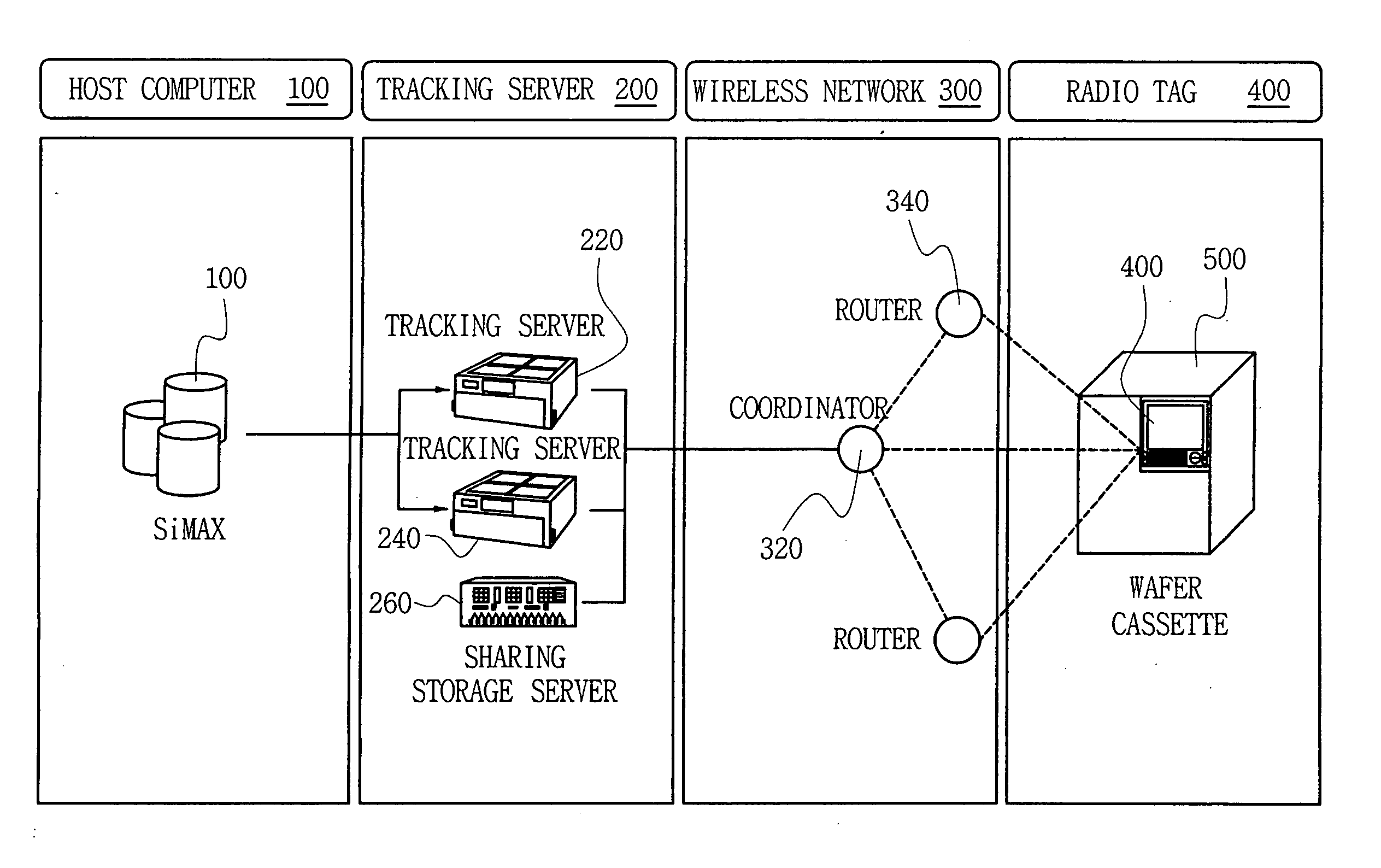
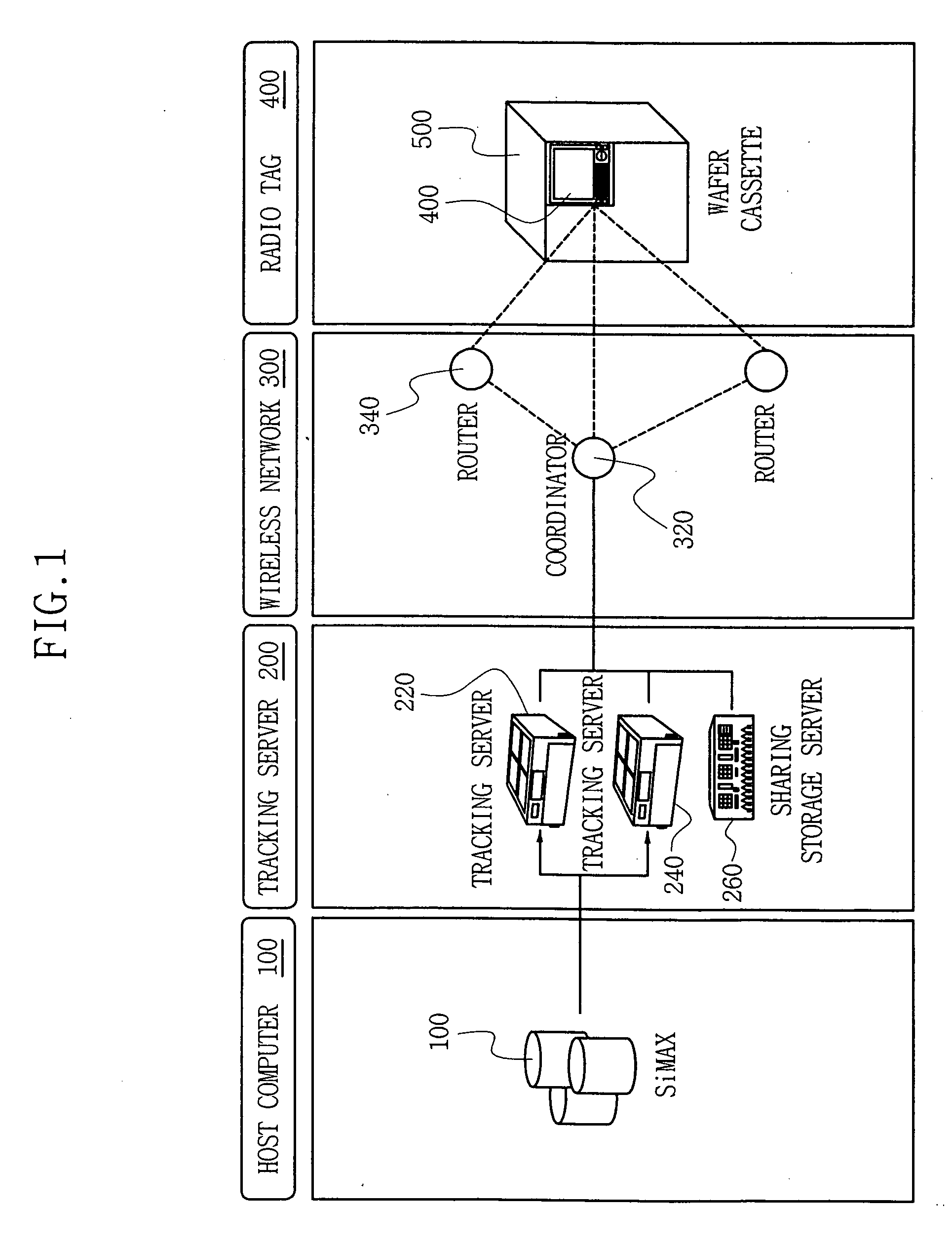
[0027]FIG. 1 shows an exemplary management system for semiconductor manufacturing equipment comprising a host computer 100 adapted to control a manufacturing process for semiconductor devices formed on silicon wafers. The exemplary management system also comprises a tracking server 200 adapted to recognize and estimate the status of a wafer cassette through the manufacturing process in response to a data signal received from host computer 100. In accordance with this status estimation, tracking server 200 is further adapted to determine an optimal transfer path for the cassette, and transmit this information to host computer 100.

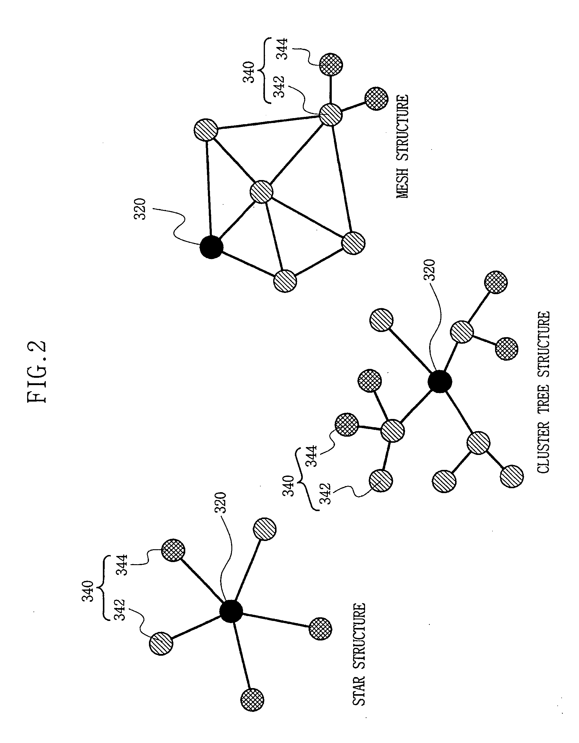
[0028] The illustrated embodiment of the management system contemplates the use of a radio ta...


PUM


Abstract

A management system for semiconductor manufacturing equipment in a manufacturing facility is provided. The system includes a host computer communicating with a tracking server, the tracking server communicating with a wireless network adapted to communicate with a radio tag associated with a wafer cassette. The tracking server is adapted to receive status information from the radio tag via the wireless network, to derive location or movement information for the wafer cassette from the status information, and to determining an optimal transfer path for the wafer cassette through the manufacturing facility.

Description

BACKGROUND OF THE INVENTION [0001] 1. Technical Field [0002] Embodiments of the invention relate to a management system for semiconductor manufacturing equipment. More particularly, embodiments of the invention relate to a management system for semiconductor manufacturing equipment capable of real-time monitoring the transfer of wafers between various pieces of semiconductor manufacturing equipment. [0003] This application claims priority to Korean Patent Application No. 10-2005-0100156 filed Oct. 24, 2005, the subject matter of which is hereby incorporated by reference in its entirety. [0004] 2. Discussion of Related Art [0005] The manufacture of semiconductor devices on silicon wafers generally involves a complex sequence of fabrication processes. Specific fabrication processes include, for example, deposition processes adapted to form material layers on a semiconductor substrate, photolithography and etching processes adapted to pattern the material layers, implantation processes...

Claims


Application Information

Patent Timeline
Patent Type & Authority Applications(United States)
IPC IPC(8): G08B13/14G06F17/00G08B5/22
CPCG05B19/4183G05B19/41855G05B2219/31095G05B2219/31162G05B2219/31281G05B2219/31286G05B2219/33199G05B2219/45031G06K2017/0045G06Q10/08G06Q50/04Y02P90/30Y02P90/02G06K17/00H04W84/18H01L21/02
Inventor PARK, JIN-WOOPARK, HONG-JINPARK, HYOUNG-MINHWANG, YOUNG-HAKPARK, YONG-BUM
Owner SAMSUNG ELECTRONICS CO LTD
Why Eureka
Try Eureka